Flow path member, heat exchanger including the flow path member, and semiconductor manufacturing apparatus including the flow path member

a technology of flow path and heat exchanger, which is applied in the direction of manufacturing tools, light and heating equipment, laminated elements, etc., to achieve the effects of high electrical reliability, low resistance, and high electrical reliability

Active Publication Date: 2015-03-26
KYOCERA CORP
View PDF8 Cites 2 Cited by
  • Summary
  • Abstract
  • Description
  • Claims
  • Application Information

AI Technical Summary

Benefits of technology

[0010]The flow path member according to the present invention includes a flow path which includes an inlet and an outlet in a base made of ceramics, and a low resistance portion whose surface resistance is less than 1×10⁷ Ω / sq in at least a part of the flow path. Accordingly, even if a fluid supplied to the flow path is charged with static electricity before being supplied, the static electricity can be removed at the low resistance portion and the electrostatic discharge can be suppressed, and thereby the flow path member with high electrical reliability can be obtained.
[0011]Further, the heat exchanger according to the present invention is formed by providing a metal plate on an upper surface or inside of the lid portion of the flow path member with high electrical reliability. Accordingly, the heat exchanger with electrical reliability and high heat exchange efficiency that withstands long-term use can be obtained.
[0012]Further, the semiconductor manufacturing apparatus according to the present invention includes the flow path member with high electrical reliability. Accordingly, the semiconductor manufacturing apparatus in which a trouble does not occur in the manufacture or inspection of a semiconductor element can be obtained.

Problems solved by technology

Then, if the static electricity is discharged when the fluid charged with the static electricity flows in the flow path member from the inlet, this causes a trouble in the manufacture or inspection of a semiconductor element.

Method used


Image

  • Flow path member, heat exchanger including the flow path member, and semiconductor manufacturing apparatus including the flow path member
  • Flow path member, heat exchanger including the flow path member, and semiconductor manufacturing apparatus including the flow path member
  • Flow path member, heat exchanger including the flow path member, and semiconductor manufacturing apparatus including the flow path member

Examples


example 1

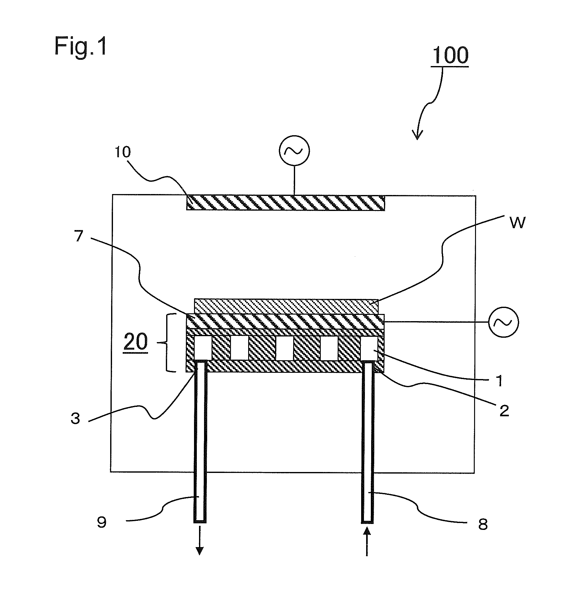
[0064]Using the semiconductor manufacturing apparatus which includes the flow path member of the embodiment illustrated in FIG. 1, a test on whether the static electricity of a fluid caused by circulating the fluid is removed or not was performed.

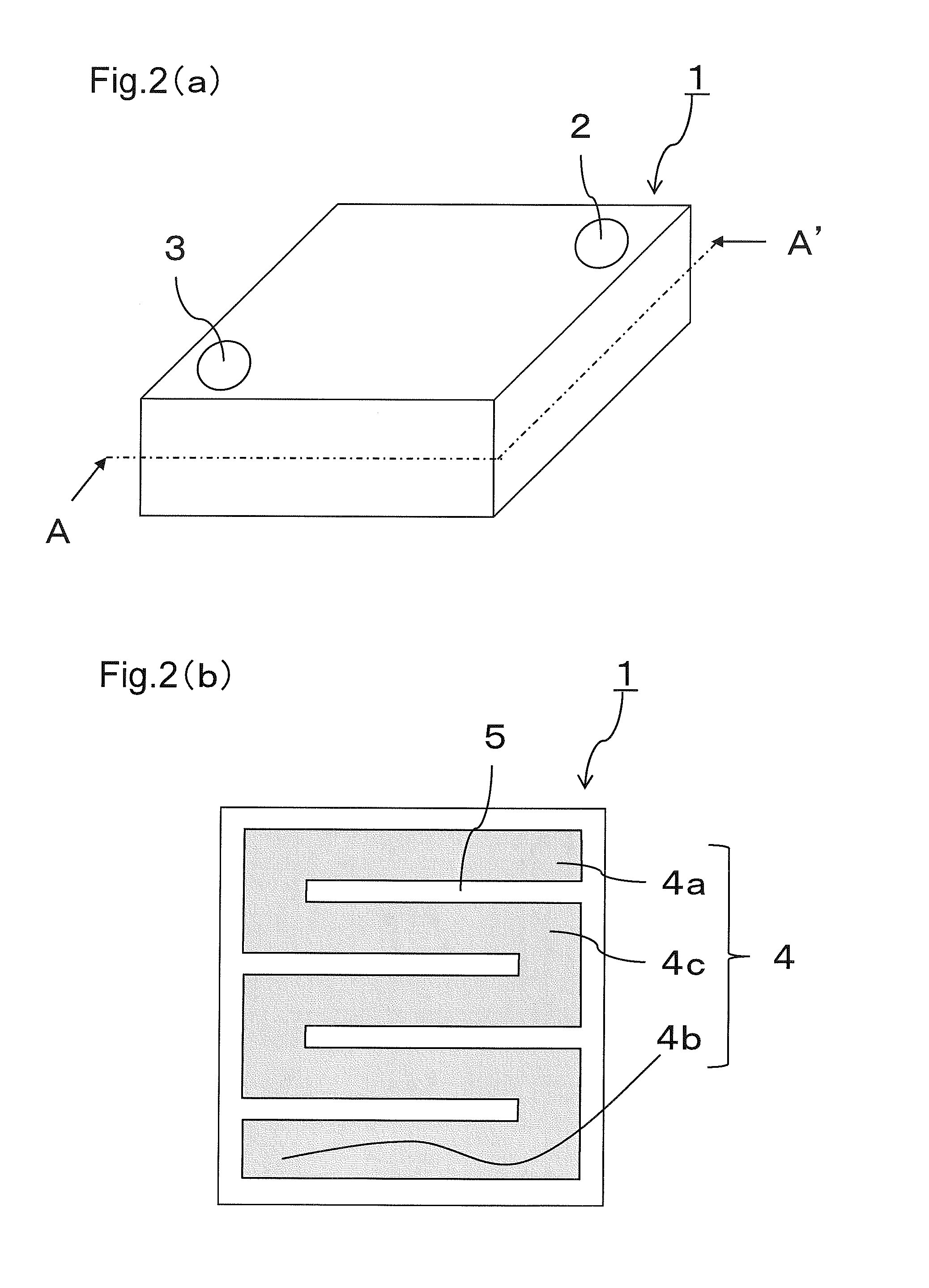
[0065]The flow path member used at this time was the flow path member illustrated in FIG. 2, and a manufacturing of the flow path member was performed by preparing silicon carbide powder whose average particle size is 1.25 μm, and powder of boron carbide and carboxylate as sintering aids, and then by weighing and mixing each powder so that boron carbide powder is 0.76 mass % and carboxylate powder is 2.2 mass % with respect to 100 mass % of silicon carbide powder.

[0066]Then, together with the mixed powder, polyvinyl alcohol as a binder, water, and a dispersing agent were put into a ball mill and were mixed to produce slurry.

[0067]Then, a molded body was obtained by using the obtained slurry to produce a plurality of green sheets by a well-k...


PUM

PropertyMeasurementUnit
particle sizeaaaaaaaaaa

Abstract

A flow path member includes a flow path which has an inlet and an outlet in a base made of ceramics, and a low resistance portion whose surface resistance is less than 1×10⁷ Ω/sq in at least a part of the flow path.

Description

TECHNICAL FIELD[0001]The present invention relates to a flow path member, and a heat exchanger and a semiconductor manufacturing apparatus which include the flow path member.BACKGROUND ART[0002]A holding table with a flow path (hereinafter, described as a flow path member) is used to hold a wafer which is a substrate material of a semiconductor element, and heating or cooling of the wafer is performed by circulating a fluid of high or low temperature in the flow path in manufacture or inspection of the semiconductor element. Ceramics have been used as a material of the flow path member, because the ceramics allow the use of a highly corrosive gas or liquid for a fluid flowing in the flow path, have good durability and corrosion resistance, and have a good insulation property.[0003]Here, the fluid which circulates in the flow path in the flow path member is supplied to an entrance (hereinafter, described as an inlet) of the flow path through a tube or the like; however, not a small a...

Claims


Application Information

Patent Timeline
Patent Type & Authority Applications(United States)
IPC IPC(8): H01L21/683F28F21/04F28F13/18
CPCH01L21/6833F28F21/04F28F13/18H01L21/67109F28F3/12F28D7/04
Inventor SEKIGUCHI, KEIICHIFUJIO, KAZUHIKOISHIMINE, YUUSAKU
Owner KYOCERA CORP
Why Eureka
Try Eureka