
Oxide thin film transistor and method of fabricating the same

a thin film transistor and thin film technology, applied in the field of tft, can solve the problems of low mobility, failure to meet the constant current bias condition, difficult to have a large area, and requiring a high temperature process, so as to minimize contact resistance, simplify the process, and ensure the effect of stability

Active Publication Date: 2014-11-20
LG DISPLAY CO LTD
View PDF12 Cites 22 Cited by
  • Summary
  • Abstract
  • Description
  • Claims
  • Application Information

AI Technical Summary

Benefits of technology

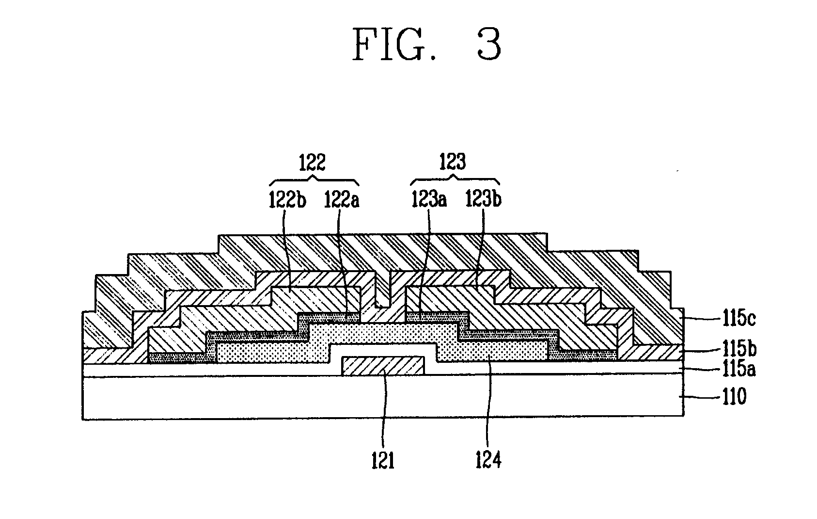
The patent text describes a new method for making oxide thin film transistors (TFTs) that prevents damage to the active layer during patterning of the source and drain electrodes. This is achieved by using a dual (double) passivation layer structure, which includes a lower layer for overcoming deficiencies and an upper layer for minimizing external influences. This improves stability and reliability of the device, while also simplifying processes and reducing device size. Overall, this method ensures stable and excellent device characteristics.

Problems solved by technology

The foregoing LCD is light and has low power consumption, as such, the LCD receives much attention, but the LCD is a light receiving device, not a light emission device, having a technical limitation in brightness, a contrast ratio, a viewing angle, and the like.
An amorphous silicon thin film transistor (TFT) used for the above-described LCD may be fabricated in a low temperature process, but has a very low mobility and fails to satisfy a constant current bias condition.
Meanwhile, a polycrystalline silicon TFT has a high mobility and satisfying constant current bias condition but fails to secure uniform characteristics, making it difficult to have a large area and requiring a high temperature process.
Here, when the oxide semiconductor is applied to a conventional bottom gate type TFT, the oxide semiconductor is damaged during etching of source and drain electrodes.
This may cause a problem in reliability of a device.
Recently, wet etching with improved selectivity is being attempted but deterioration of device characteristics is caused due to partial etching, which results from low uniformity.
Upon using the wet etching, a loss or damage of the active layer is caused due to a property of the oxide semiconductor, which is vulnerable to an etchant.
Even when the source and drain electrodes are formed using the dry etching, the active layer is denatured due to back-sputtering and oxygen deficiency of the oxide semiconductor.
Specifically, when molybdenum (Mo) based metals are applied to form the source and drain electrodes in consideration of contact resistance with the oxide semiconductor, it is difficult to develop an etchant with selectivity with respect to the oxide semiconductor which is vulnerable to acidity.
This may, however, increase the number of processes and masks, causing a decrease of mass production.

Method used


Image

  • Oxide thin film transistor and method of fabricating the same
  • Oxide thin film transistor and method of fabricating the same
  • Oxide thin film transistor and method of fabricating the same

Examples


Embodiment Construction

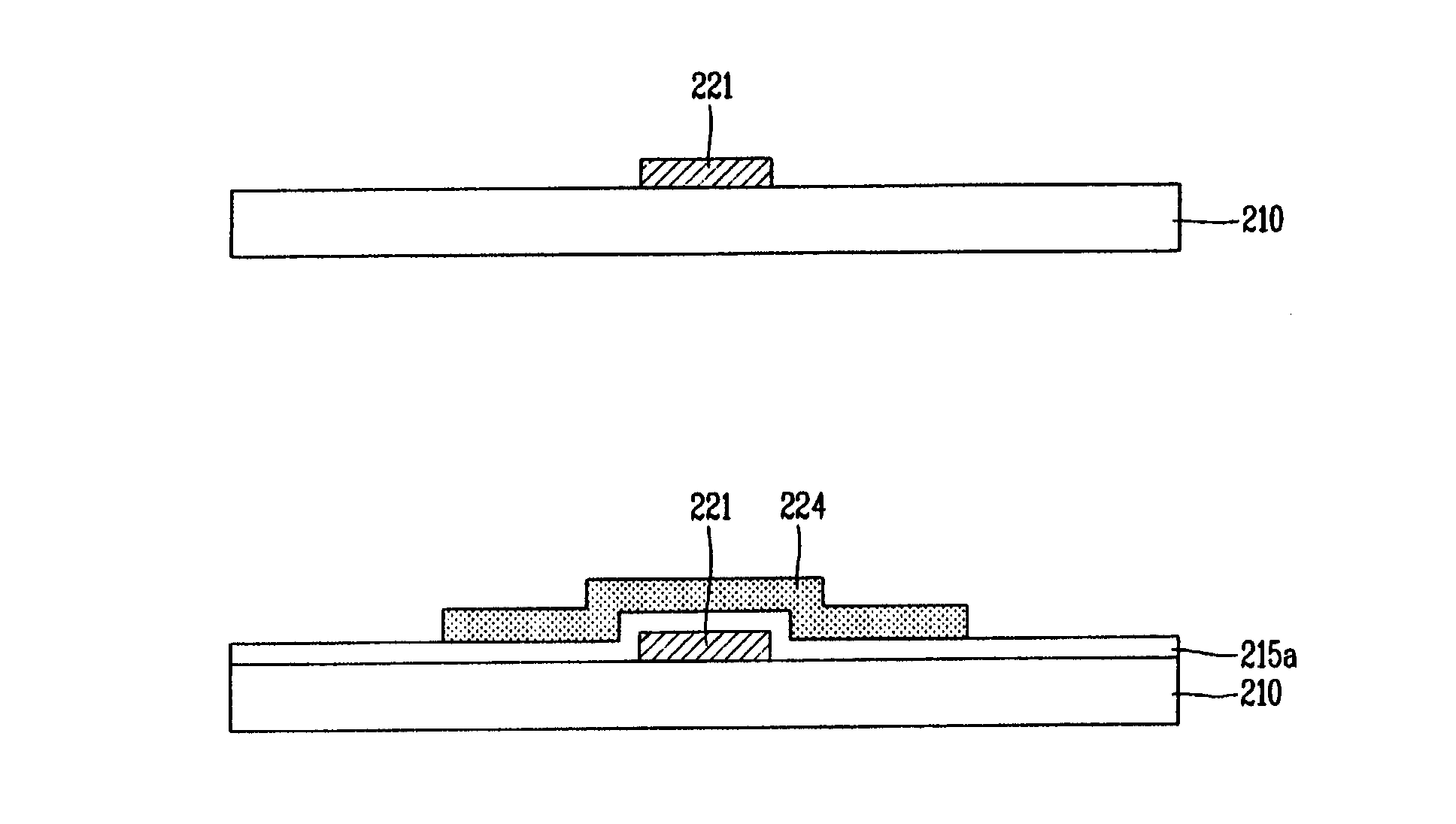
[0045]An oxide thin film transistor (TFT) and its fabrication method according to exemplary embodiments of the present disclosure will now be described with reference to the accompanying drawings, such that those skilled in the art to which the present disclosure belongs can easily practice it.

[0046]Advantages and features of the present disclosure and methods for achieving those will be obviously understood by the following exemplary embodiments described in detail with reference to the accompanying drawings. However, the present disclosure is not to be construed as being limited to the exemplary embodiments but can be implemented into various forms. The exemplary embodiments of the present disclosure are merely illustrated to fully describe the present disclosure and provided to help a skilled person in the art to understand the scope of the present disclosure. The present disclosure is merely defined by the claims. The same / like reference symbols or numerals over the specificatio...


PUM


Abstract

The present disclosure relates to an oxide thin film transistor and a fabricating method thereof. In the oxide thin film transistor, which uses amorphous zinc oxide (ZnO) semiconductor as an active layer, damage to the oxide semiconductor due to dry etching may be minimized by forming source and drain electrodes in a multilayered structure having at least two layers, and improving stability and reliability of a device by employing a dual passivation layer structure, which includes a lower layer for overcoming a deficiency and an upper layer for minimizing external affection, on the multilayered source and drain electrodes.

Description

CROSS-REFERENCE TO RELATED APPLICATIONS[0001]This application claims the benefit of the Korean Patent Application No. 10-2013-0054551 filed on May 14, 2013 which is hereby incorporated by reference for all purposes as if fully set forth herein.BACKGROUND OF THE INVENTION[0002]1. Field of the Invention[0003]The present disclosure relates to an oxide thin film transistor (TFT) and a fabrication method thereof. More particularly, the present invention relates to an oxide TFT having an amorphous zinc oxide semiconductor as an active layer, and a fabrication method thereof.[0004]2. Discussion of the Related Art[0005]As the consumers' interest in information displays is growing and the demand for portable (mobile) information devices is increasing, research and commercialization of light and thin flat panel displays (FPD), which substitute cathode ray tubes (CRTs), the conventional display devices, have increased. Among FPDs, the liquid crystal display (LCD) is a device for displaying ima...

Claims


Application Information

Patent Timeline
Patent Type & Authority Applications(United States)
IPC IPC(8): H01L29/786H01L29/66
CPCH01L29/78636H01L29/78693H01L29/66969H01L29/78606H01L29/45H01L29/66742
Inventor BAE, JONGUK
Owner LG DISPLAY CO LTD
Learn More