
Methods and Systems for Clocking a Physical Layer Interface

Active Publication Date: 2014-10-23
SYNOPSYS INC
View PDF10 Cites 6 Cited by
  • Summary
  • Abstract
  • Description
  • Claims
  • Application Information

AI Technical Summary

Benefits of technology

This patent text describes methods and systems for improving the performance of a computing device by reducing latency and optimizing the distribution of clock and reset signals. These improvements aim to reduce chip area usage and power consumption, leading to more efficient and effective computing.

Problems solved by technology

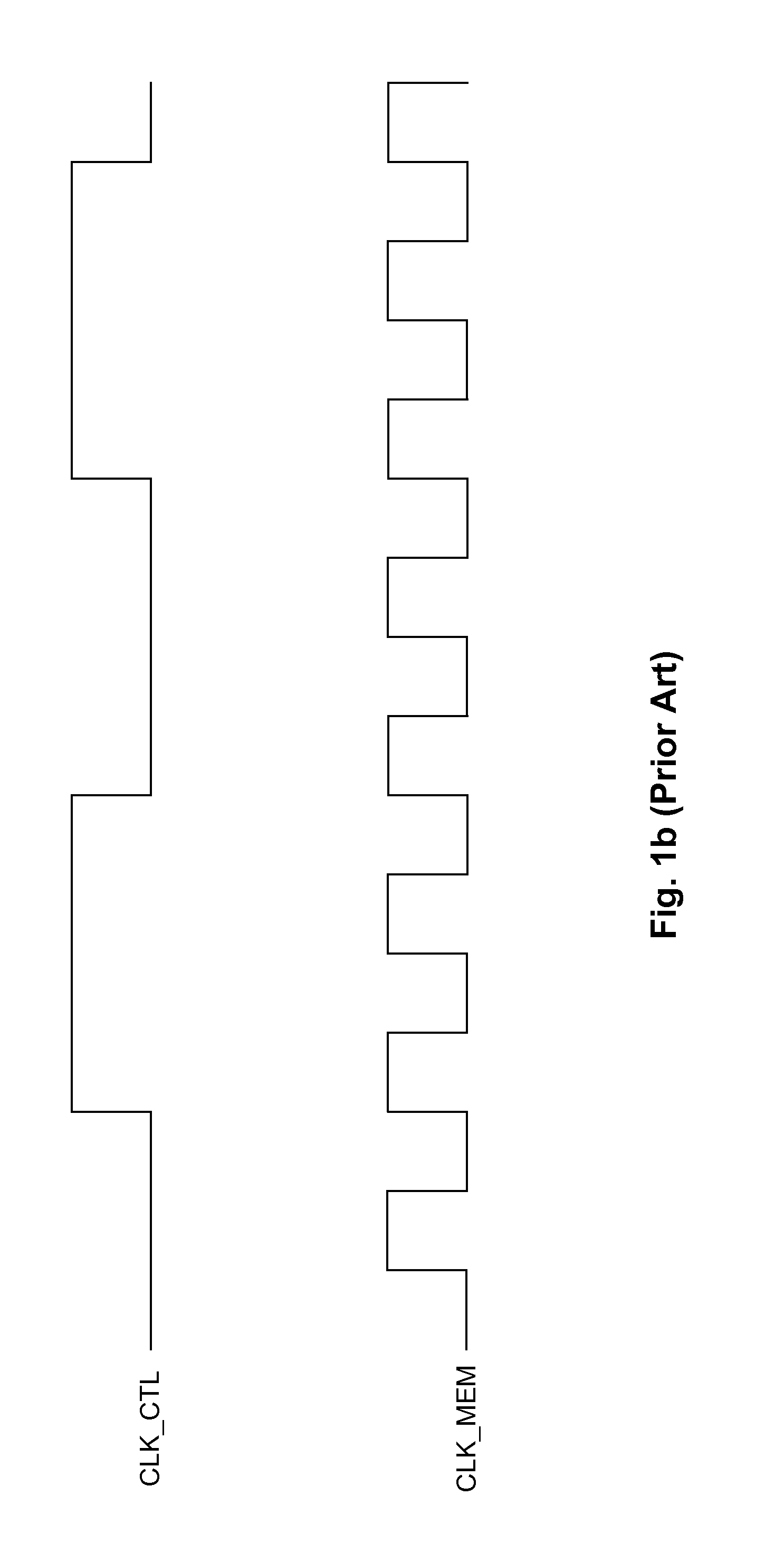
Thus, there is uncertainty as to alignment of the clock signals.
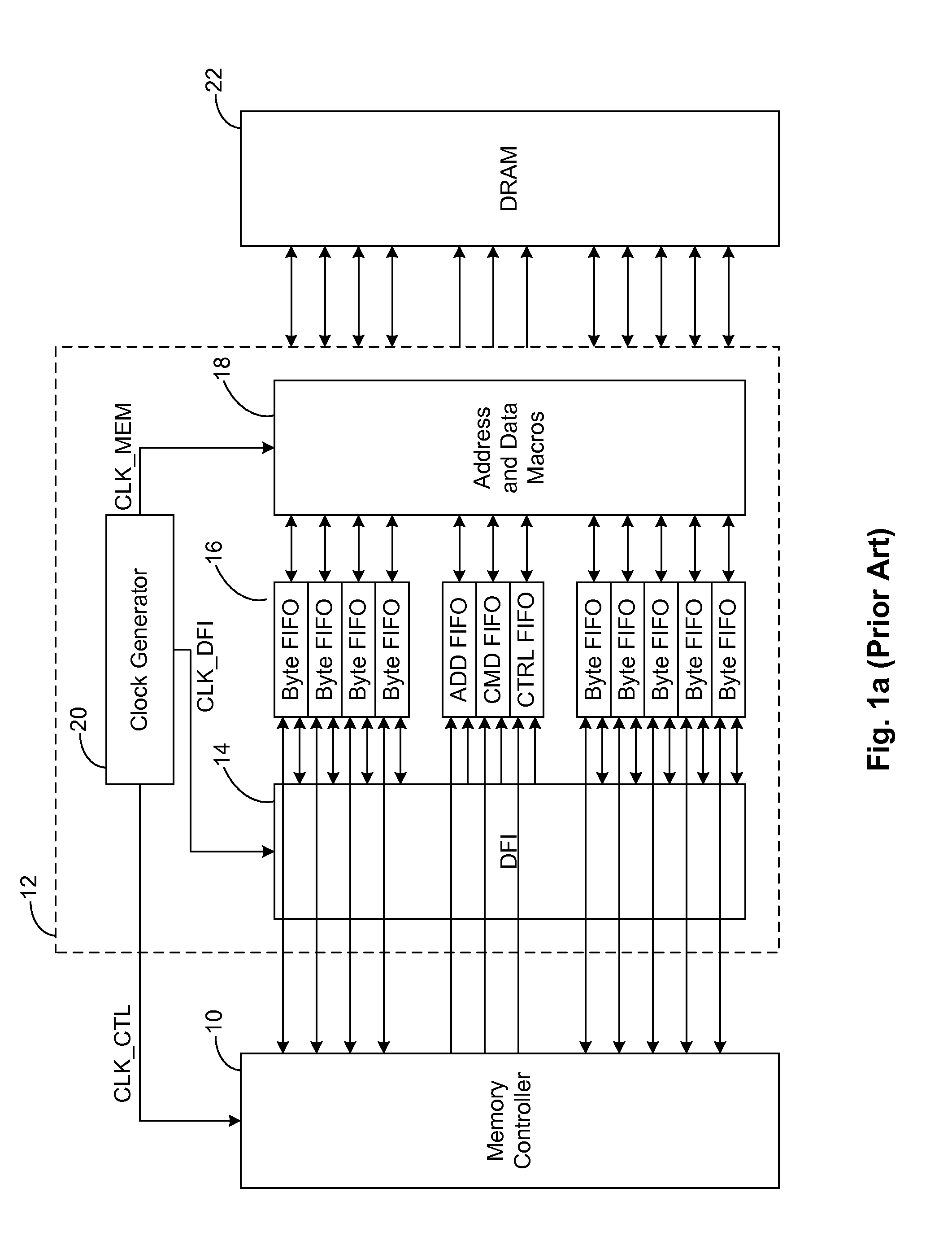
The depths of logic in the PHY 12 and in the memory controller 10 are different, and, moreover, the logic may be operating at integral multiple frequencies, which prove to be challenging during integration.
Additionally, the minimum latency for reliable operation needs at least three additional cycles of CLK_MEM due to a clock domain crossing, which will increase the overall latency of the system and also increase the needed chip area.
Due to its relatively extensive depth and length, clock distribution in the DDR macro is challenging in itself, and further difficult when trying to synchronize the signals for the DDR macro.
Unfortunately, the second distribution network 26 consumes a great amount of chip area and consumes a great amount of power.

Method used


Image

  • Methods and Systems for Clocking a Physical Layer Interface
  • Methods and Systems for Clocking a Physical Layer Interface
  • Methods and Systems for Clocking a Physical Layer Interface

Examples


Embodiment Construction

[0035]In the following detailed description of the embodiments, reference is made to the accompanying drawings, which form a part hereof, and in which is shown by way of illustration of specific embodiments in which the present invention may be practiced.

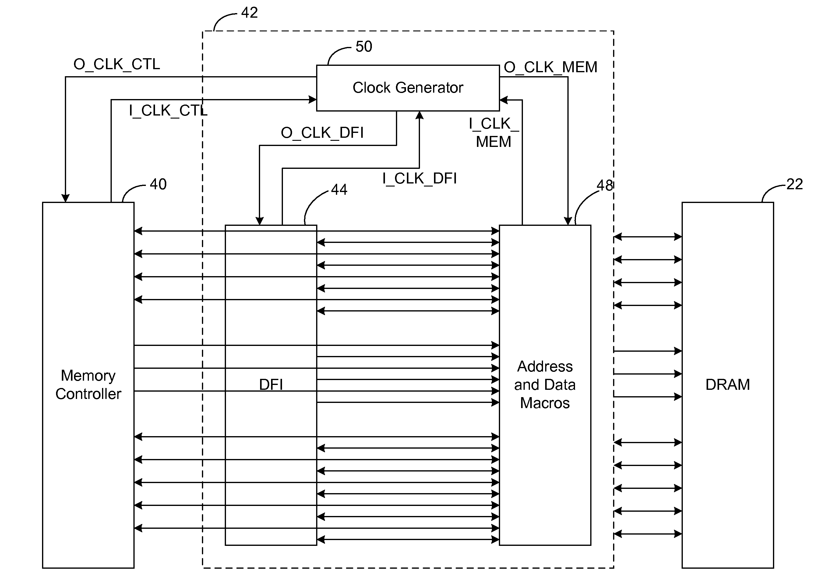
[0036]Generally, the present invention provides methods and systems for synchronizing various clock signals used in a PHY and a memory controller of a computing device. Synchronization can include phase alignment along the respective rising edges (or the respective falling edges) of a plurality of signals to be synchronized. Thereby, the need for clock domain crossing synchronization can be eliminated.

[0037]FIG. 2a illustrates a diagram of the present invention for interfacing a memory controller and an external memory via a PHY. A PHY 42 comprises a clock generator 50, a DFI block 44, and address and data macros 48 for communicating between the PHY 42 and a DRAM 22. The clock generator 50 generates clock signals for clocking a memo...


PUM


Abstract

A method for clocking a physical layer (“PHY”) and a controller of a computing device, comprises the steps of: generating a reference clock signal; synchronizing a plurality of clock signals as a function of the reference clock signal; and clocking the controller and the PHY using the plurality of synchronized clock signals.

Description

CROSS REFERENCE [0001]This application claims priority from a provisional patent application entitled “Apparatuses, Methods, and Systems Using Integrated Circuits” filed on Apr. 19, 2013 and having an Application No. 61 / 814,153. Said application is incorporated herein by reference.FIELD OF INVENTION [0002]This invention generally relates to methods and systems for a physical layer interface of a computing device and, in particular, to methods and systems for clock generation and synchronization for a physical layer interface of a computing device.BACKGROUND [0003]A physical layer of a computing device (“PHY”) is used for communicating between integrated circuits and external devices, such as other integrated circuits, typically through a data bus or a set of signal wires. The physical layer is typically configured to implement a desired communication protocol or specification that has been established for the particular application.[0004]FIG. 1a illustrates a diagram of a physical l...

Claims


Application Information

Patent Timeline
IPC IPC(8): H04L7/00
CPCH04L7/0012H03L7/00G06F1/04G06F1/10G06F1/28H03K19/0175H03K19/017509H03L7/0802H03L7/093H04L25/0276H04L25/028G06F13/385Y02D10/00G06F1/08G06F1/14G06F1/06G06F1/12
Inventor CHALASANI, PRASADRAO, VENKATA N.S.N.
Owner SYNOPSYS INC
Learn More