Component-Embedded Substrate Manufacturing Method and Component-Embedded Substrate Manufactured Using the Same

a technology of embedded substrates and manufacturing methods, which is applied in the direction of printed circuit aspects, printed circuit non-printed electric components association, and semiconductor/solid-state device details, etc., can solve the problems of reducing the reliability of connection portions, and achieve the effect of ensuring the integrity of the connection portion, and constant thickness of the adhesive layer

Inactive Publication Date: 2014-10-09
MEIKO ELECTRONICS CO LTD
View PDF0 Cites 12 Cited by
  • Summary
  • Abstract
  • Description
  • Claims
  • Application Information

AI Technical Summary

Benefits of technology

The present invention provides a component-embedded substrate manufacturing method that allows for high accuracy in positioning the component and its connection to the terminal of the metal layer. The method achieves this by using a main mark and a secondary mark formed simultaneously with a seat formed at the same time. The seat acts as a spacer to maintain a constant thickness of the adhesive layer between the component and the metal layer. The via hole is formed at the exact position in relation to the terminal of the component. The method also allows for the use of a wider range of adhesives and increases production efficiency. The obtained substrate has high accuracy in positioning and low occurrence of defective products.

Problems solved by technology

Therefore, the connection portions inside the insulating substrate in the component-embedded substrate disclosed in Patent Document 1 are heated to a solder melting temperature several times, which may reduce the reliability of the connection portions.
Specifically, the melting point of the copper is higher than the melting point of the solder, and thus the component-embedded substrate placed in the reflow furnace does not allow the connection portions to melt, thereby maintaining the reliability of the connection portions.

Method used


Image

  • Component-Embedded Substrate Manufacturing Method and Component-Embedded Substrate Manufactured Using the Same
  • Component-Embedded Substrate Manufacturing Method and Component-Embedded Substrate Manufactured Using the Same
  • Component-Embedded Substrate Manufacturing Method and Component-Embedded Substrate Manufactured Using the Same

Examples


Embodiment Construction

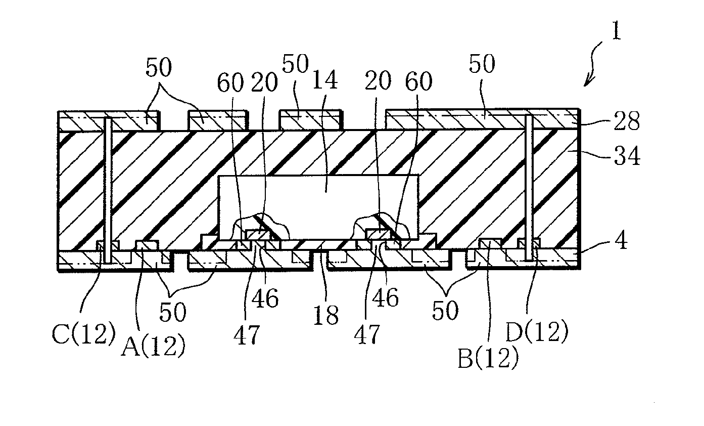
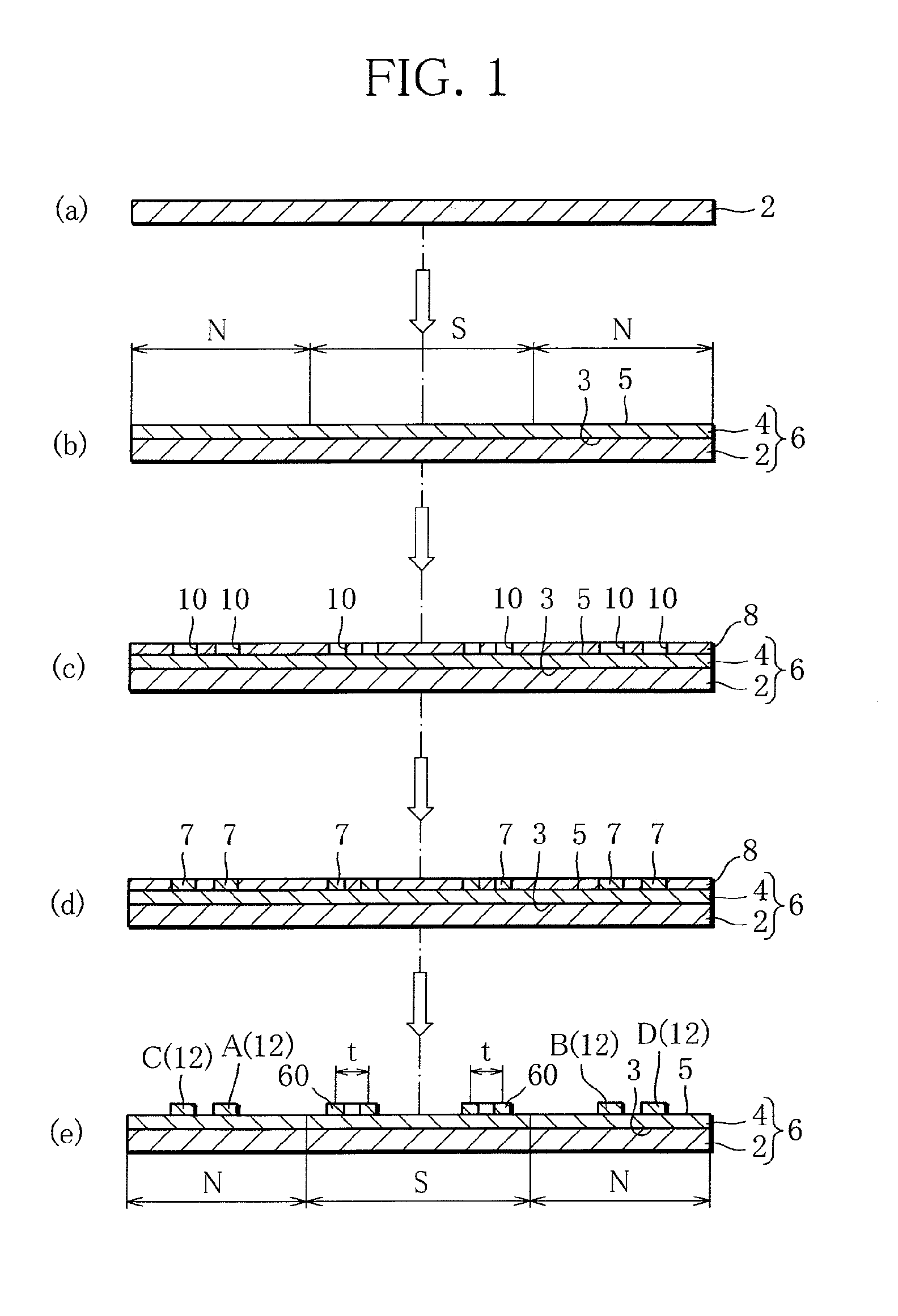
[0040]There follows a description of a procedure for manufacturing a component-embedded substrate having an electronic component (hereinafter referred to as an intra-substrate component) 14 embedded in an insulating substrate by applying a component-embedded substrate manufacturing method of the present invention thereto.

[0041]According to the present invention, first, a metal layer is formed on a support plate (metal layer forming step).

[0042]As illustrated in FIG. 1(a), the present step prepares a support plate 2. The support plate 2 is, for example, a thin plate made of stainless steel. Then, as illustrated in FIG. 1(b), a first metal layer 4 made of a thin film is formed on the support plate 2. The first metal layer 4 is made of, for example, a copper plating film obtained by electroplating. Thus, a copper-clad steel plate 6 is obtained. Here, a surface of the first metal layer 4 contacting the support plate 2 is assumed to be a first surface 3; and a surface opposite to the fir...


PUM

PropertyMeasurementUnit
conductiveaaaaaaaaaa
densityaaaaaaaaaa
insulatingaaaaaaaaaa

Abstract

The method includes forming an annular seat and main marks on a metal layer simultaneously so that the annular seat opposes with a terminal of an electronic component when the component is placed above the annular seat at a subsequent step; then positioning the electronic component in a mounting expected region using the main marks and mounting the electronic component with an adhesive layer therebetween; then burying the electronic component and the main marks in an insulating substrate; then removing part of the metal layer and thereby forming first and second windows; then irradiating the adhesive layer with laser using the exposed main marks thereby forming a laser via hole; and then filling the laser via hole with copper and forming a wiring pattern from the metal layer electrically connected to the terminal through a conductive via.

Description

TECHNICAL FIELD [0001]The present invention relates to a component-embedded substrate manufacturing method for embedding electrical or electronic components in a substrate and a component-embedded substrate manufactured using the same.BACKGROUND ART [0002]Recently, with increased density of components mounted on the surface of an electronic circuit board, that is, enhanced functionality of the electronic circuit board, attention has been paid to a component-embedded substrate having a structure in which electronic components are embedded in an insulating substrate serving as an insulating layer. A wiring pattern is formed on the surface of the insulating substrate of the component-embedded substrate. The component-embedded substrate on the surface of which other various electronic components are mounted at a predetermined position of the wiring pattern can be used as a module board. In addition, the component-embedded substrate can also be used as a core board for use in manufacturi...

Claims


Application Information

Patent Timeline
Patent Type & Authority Applications(United States)
IPC IPC(8): H05K13/04H05K1/18
CPCH05K1/184H05K13/0469Y10T29/49135H05K2203/1469H05K3/007H05K1/188H05K2201/09918H05K3/4602H05K2203/167H01L2224/83005H01L2224/83132H01L21/568H01L23/544H01L24/24H01L24/82H01L24/83H01L2224/04105H01L2224/32245H01L2224/82039H01L2224/8314H01L2224/83192H01L2224/92144H01L23/49827H01L21/4846H01L23/5389H01L24/19H01L24/27H01L24/29H01L24/32H01L24/92H01L2224/2741H01L2224/27436H01L2224/2919H01L2224/2929H01L2224/29387H01L2924/14H01L2224/82132H01L2223/54426H01L2223/54486H01L23/145
Inventor IMAMURA, YOSHIO
Owner MEIKO ELECTRONICS CO LTD
Why Eureka
Try Eureka