
NAND Flash Memory

a technology memory density, applied in the field of digital memory devices, can solve the problems of compromising the usefulness of high-performance sequential, not offering command compatibility with serial nor flash memory, and high density of nand flash memory cost structur

Active Publication Date: 2014-09-18
WINBOND ELECTRONICS CORP
View PDF4 Cites 44 Cited by
  • Summary
  • Abstract
  • Description
  • Claims
  • Application Information

AI Technical Summary

Benefits of technology

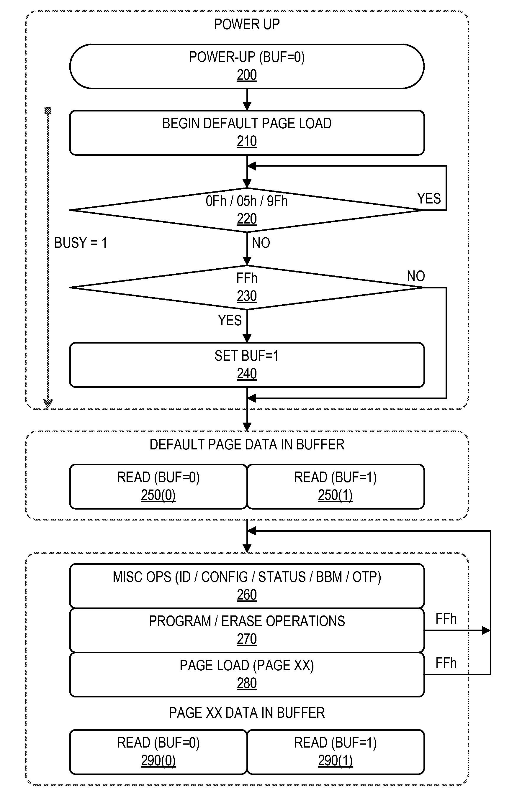
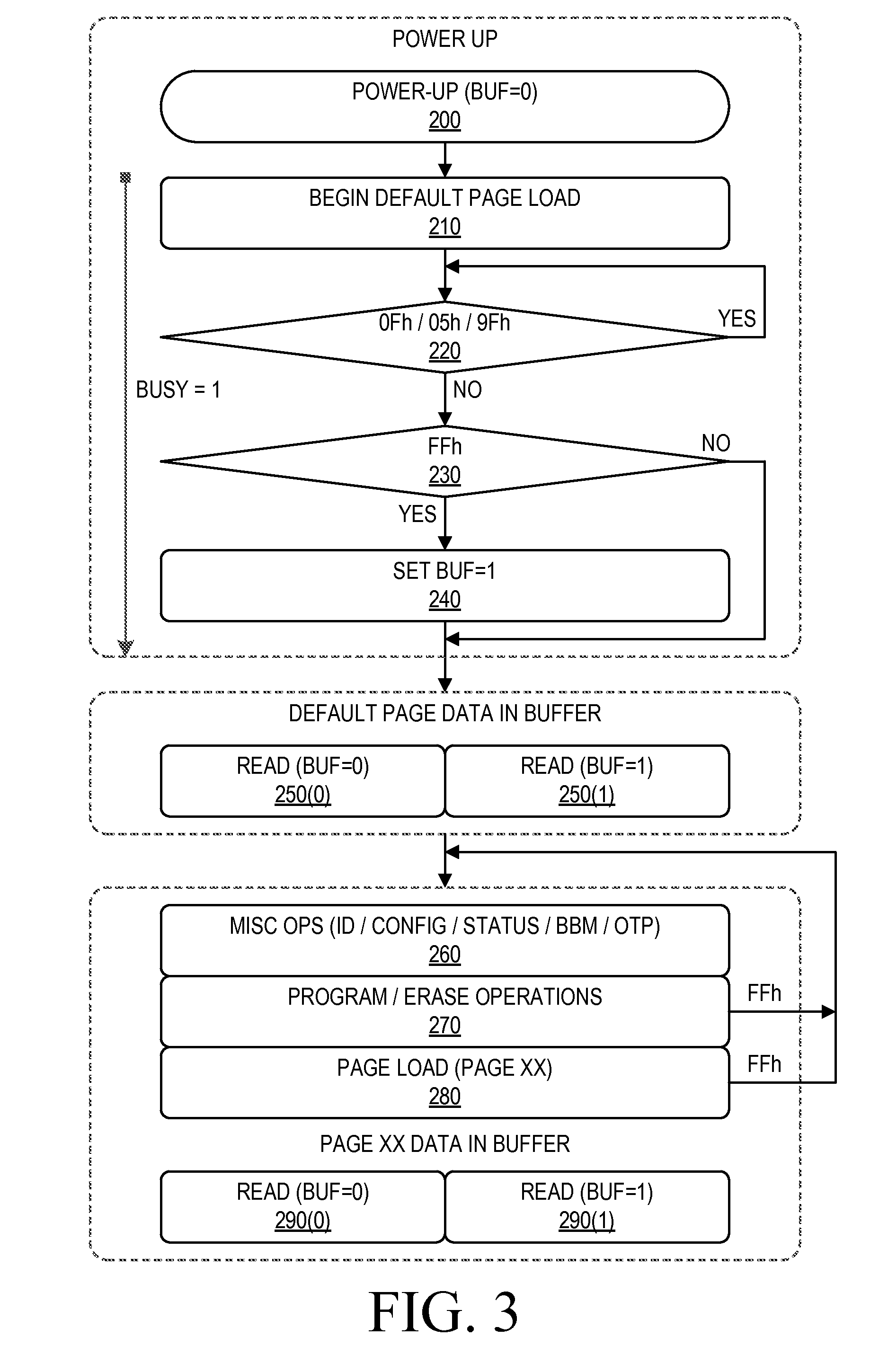
The present invention provides a serial NAND flash memory that can accept serial NOR flash memory commands and is compatible with existing serial NOR flash memory controllers. The serial NAND flash memory offers cost savings and can be used for code shadowing applications. The serial NAND flash memory device includes a package, a NAND flash memory array, a page buffer, and control logic for providing a continuous data output across page boundaries and from logically contiguous memory locations without wait intervals. The method of operating the memory device involves selecting a page of the NAND flash memory array, storing data from the selected page in the page buffer, performing ECC computations on the data, and outputting the data from the page buffer. The method can be performed automatically during power-up of the flash memory. The present invention provides a more efficient and flexible solution for code shadowing applications compared to existing solutions.

Problems solved by technology

While serial NOR flash memory is a popular solution for code shadowing applications, the cost structure at higher densities is not favorable when compared with the cost structure for NAND flash memory.
While serial NAND flash memory has been introduced, it has architectural, performance and bad block limitations that compromise its usefulness for high performance sequential and continuous code shadowing, and does not offer command compatibility with serial NOR flash memory.

Method used


Image

  • NAND Flash Memory
  • NAND Flash Memory
  • NAND Flash Memory

Examples


Embodiment Construction

[0032]High Performance serial flash memory which uses NOR memory array technology (“HPSF-NOR”) such as types W25Q64CV and W25Q128FV available from Winbond Electronics Corporation of San Jose, Calif., USA, and described in, for example, various data sheets such as Winbond Electronics Corporation, W25Q64CV SpiFlash 3V 64M-Bit Serial Flash Memory with Dual and Quad SPI, Revision F, May 7, 2012, and Winbond Electronics Corporation, W25Q128FV SpiFlash 3V 128M-Bit Serial Flash Memory with Dual / Quad SPI & QPI, Revision D, Oct. 1, 2012, which hereby are incorporated herein in their entirety by reference thereto, has certain read characteristics which render the HPSF-NOR memory particularly suitable for applications involving code shadowing (transference of executable code or data such as parameters, text, images, audio, and so forth), which are common in such electronic devices and systems as digital televisions, set-top boxes, personal computers, DVD players, networking equipment and autom...


PUM


Abstract

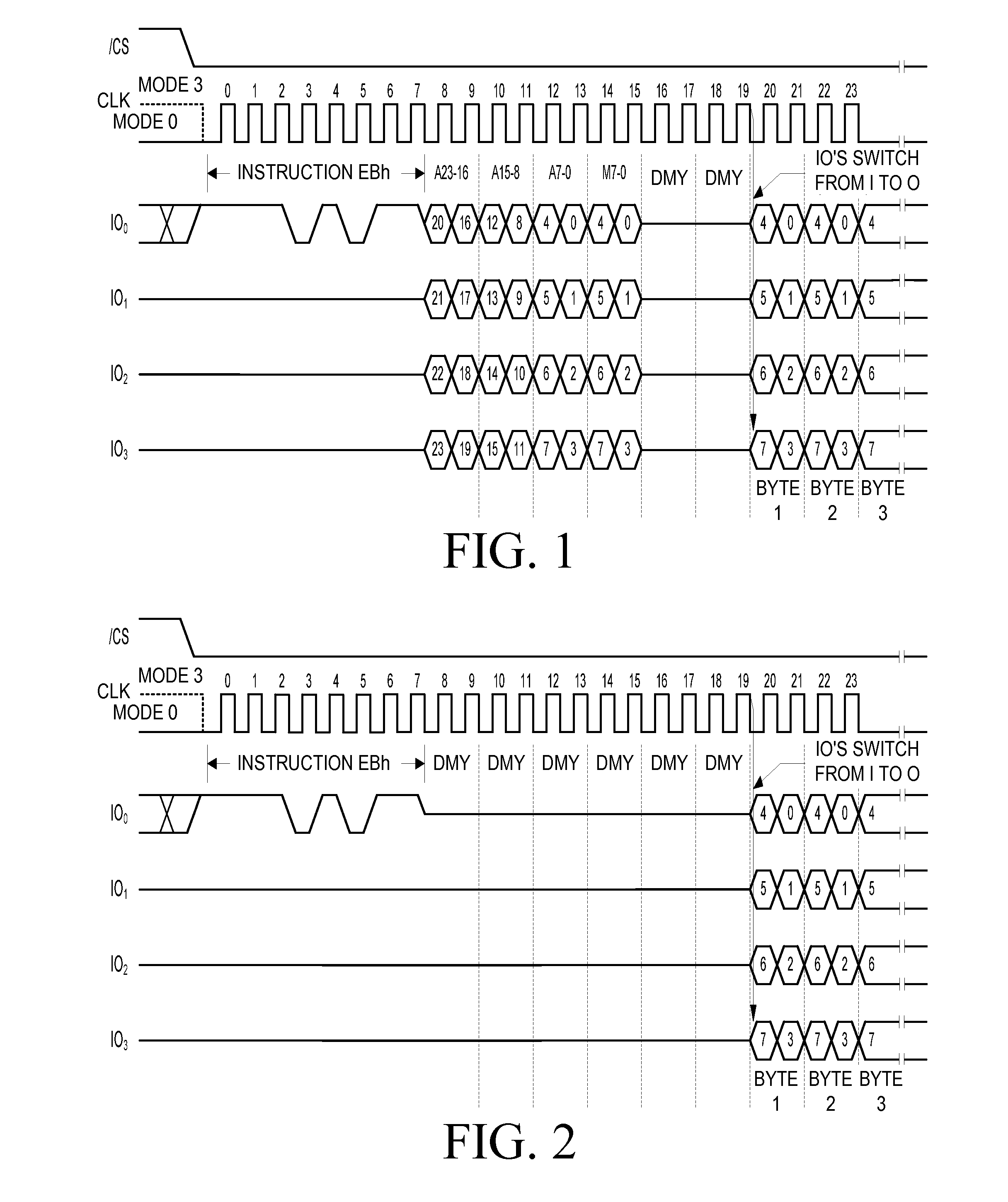
Serial NAND flash memory may be provided with the characteristics of continuous read of the memory across page boundaries and from logically contiguous memory locations without wait intervals, while also being clock-compatible with the high performance serial flash NOR (“HPSF-NOR”) memory read commands so that the serial NAND flash memory may be used with controllers designed for HPSF-NOR memory. Serial NAND flash memory having these compatibilities is referred to herein as high-performance serial flash NAND (“SPSF-NAND”) memory. Since devices and systems which use HPSF-NOR memories and controllers often have extreme space limitations, HPSF-NAND may also be provided with the same physical attributes of low pin count and small package size of HPSF-NOR memory for further compatibility. HPSF-NAND memory is particularly suitable for code shadow applications, even while enjoying the low “cost per bit” and low per bit power consumption of a NAND memory array at higher densities.

Description

BACKGROUND OF THE INVENTION[0001]1. Field of the Invention[0002]The present invention relates to digital memory devices, and more particularly to NAND flash memory having physical attributes, read command clocking characteristics, and / or read output characteristics compatible with high performance serial NOR flash memory.[0003]2. Description of Related Art[0004]Serial NOR flash memory has become a popular alternative to conventional parallel NOR flash memory. Serial NOR flash memories offer several advantages including; lower pin-count, smaller packages, simpler printed circuit boards, lower power, comparable performance and reduced device and system-level costs. Today, serial NOR flash memories are offered in densities from 512 Kilobit to 1 Gigabit, and employ the popular Serial Peripheral Interface (“SPI”).[0005]Single-bit SPI uses four pins for transferring commands, address and data to, and data from, the serial flash memory, namely: Chip Select ( / CS), Clock (CLK), Data In (DI) ...

Claims


Application Information

Patent Timeline
Patent Type & Authority Applications(United States)
IPC IPC(8): G11C16/06G11C29/04
CPCG11C29/04G11C16/06G11C2029/0411G06F11/1068G11C16/20G11C16/26G11C16/3404G06F3/0619G06F3/064G06F3/0656G06F3/0679G11C29/52
Inventor JIGOUR, ROBIN JOHNCHEN, HUIMICHAEL, ORON
Owner WINBOND ELECTRONICS CORP
Learn More