
Microwave plasma reactors and substrates for synthetic diamond manufacture

a technology of plasma reactor and substrate, which is applied in the direction of crystal growth process, polycrystalline material growth, transportation and packaging, etc., can solve the problems of dc arc plasma, disadvantages of electrode-based methods, and reliant on relatively expensive feed gases. cost in terms of kwh of energy that can be extracted

Active Publication Date: 2014-08-21
ELEMENT SIX LTD
View PDF0 Cites 9 Cited by
  • Summary
  • Abstract
  • Description
  • Claims
  • Application Information

AI Technical Summary

Benefits of technology

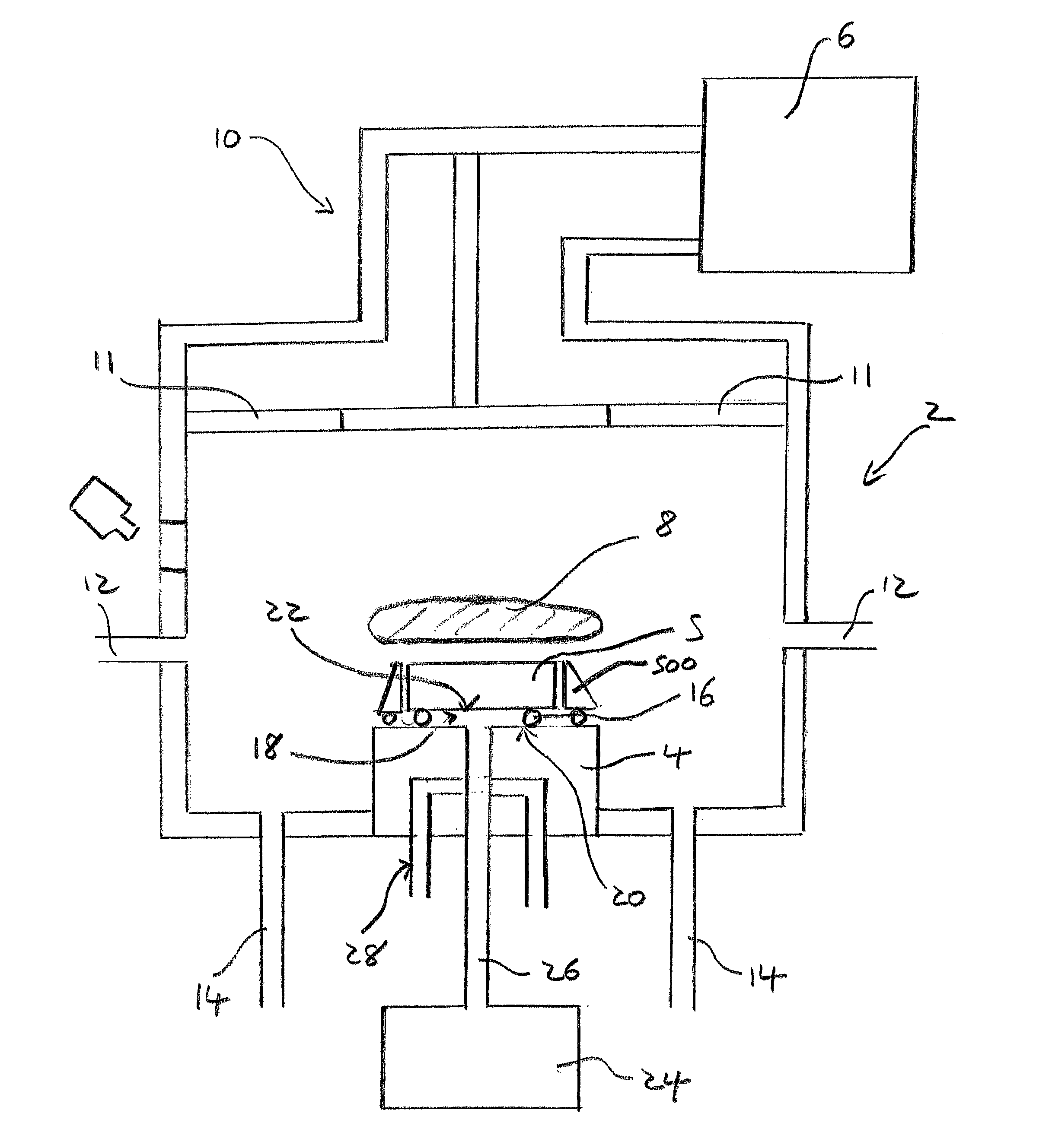
The present invention relates to a microwave plasma reactor for manufacturing synthetic diamond material using chemical vapor deposition. The reactor includes a microwave generator, a plasma chamber with a base, top plate, and side wall, and a substrate holder for supporting a substrate. The substrate is placed in the plasma chamber and the microwaves are fed into the chamber through a microwave coupling. A gas flow system is used to feed and remove process gases. The substrate is held in the plasma chamber and a microwave electric field is generated across the substrate. The substrate is disposed in a way that a localized axisymmetric electric field is created across the substrate. The reactor is designed to produce a polycrystalline diamond wafer with a flat growth surface and no cracks. The technical effects of the invention include improved quality and efficiency of synthetic diamond material production.

Problems solved by technology

Methods that involve electrodes, such as DC arc plasmas, can have disadvantages due to electrode erosion and incorporation of material into the diamond.
Combustion methods avoid the electrode erosion problem but are reliant on relatively expensive feed gases that must be purified to levels consistent with high quality diamond growth.
Also the temperature of the flame, even when combusting oxy-acetylene mixes, is insufficient to achieve a substantial fraction of atomic hydrogen in the gas stream and the methods rely on concentrating the flux of gas in a localized area to achieve reasonable growth rates.
Perhaps the principal reason why combustion is not widely used for bulk diamond growth is the cost in terms of kWh of energy that can be extracted.
Compared to electricity, high purity acetylene and oxygen are an expensive way to generate heat.
Hot filament reactors while appearing superficially simple have the disadvantage of being restricted to use at lower gas pressures which are required to ensure relatively effective transport of their limited quantities of atomic hydrogen to a growth surface.
One problem with using silicon as a substrate for CVD diamond growth in a microwave plasma growth process is power absorption by the silicon at high temperatures, leading to thermal runaway and fracture.
Another problem is that silicon is readily incorporated into CVD diamond during growth, being particularly visible as the 737 nm Si—V defect.
As such, the use of a silicon substrate can detrimentally affect the purity of the CVD diamond product.
Yet another problem is that after growth of a CVD diamond wafer on a silicon substrate, recovery of the CVD diamond wafer may require, for example, one of mechanical or acid removal.
These additional processing steps increase the time and expense of an industrially implemented process.
Despite this, the present inventors have experienced a number of problems when using such substrates.
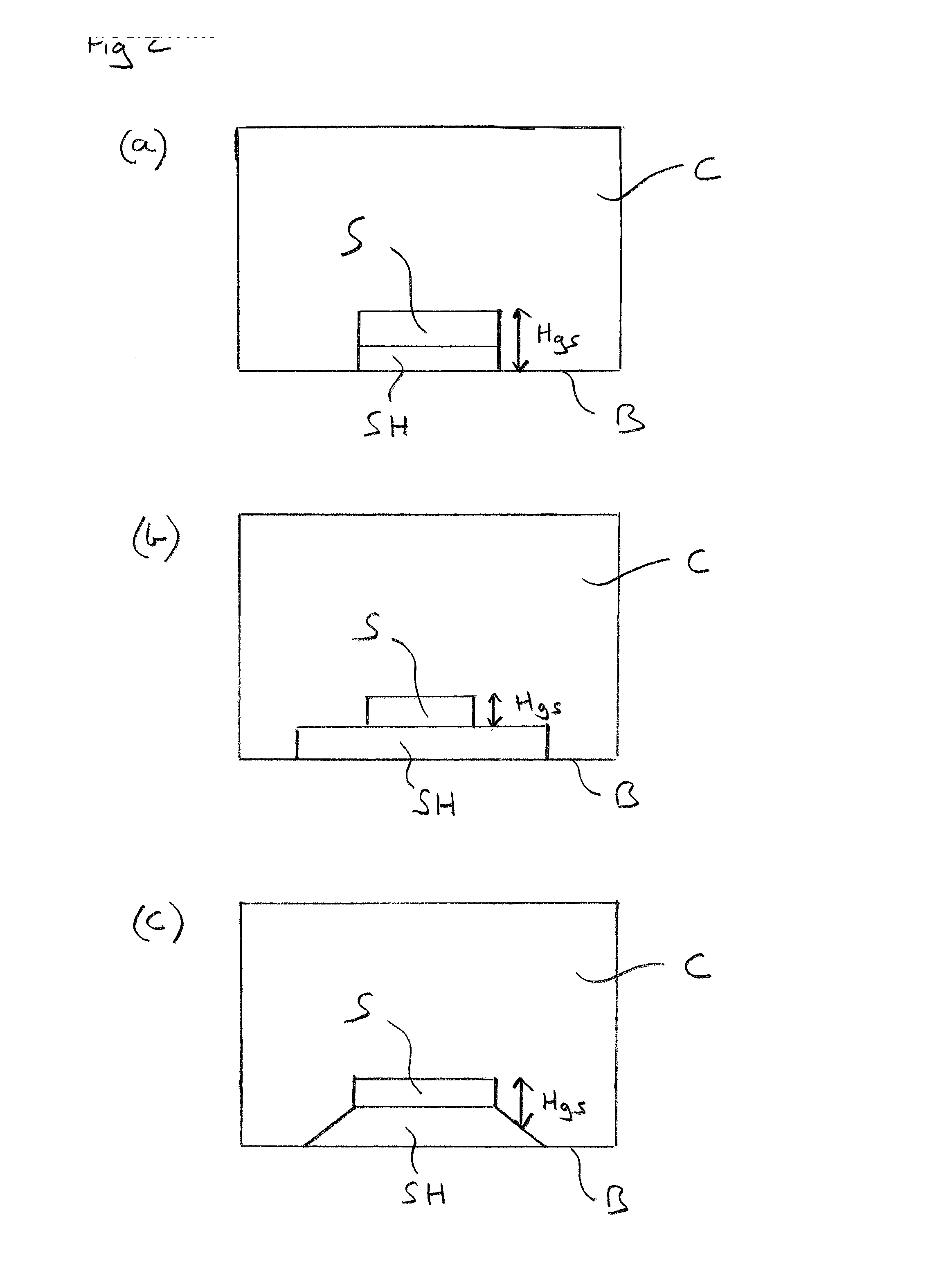
These problems tend to be exacerbated when larger substrates are used for growing large area polycrystalline diamond discs (e.g. 80 mm diameter or more) or when growing a plurality of single crystal diamonds in a single growth run on a plurality of single crystal diamond substrates adhered to a refractory metal substrate over a relatively large area (e.g. 80 mm diameter or more).
This is particularly problematic as there is an on going need to increase the area over which high quality, uniform CVD diamond can be grown.
Furthermore, these problems tend to be exacerbated when the substrates are reused in subsequent growth runs.
This is particularly problematic as the substrates are expensive and reuse is desirable in an economically competitive industrial process.

Method used


Image

  • Microwave plasma reactors and substrates for synthetic diamond manufacture
  • Microwave plasma reactors and substrates for synthetic diamond manufacture
  • Microwave plasma reactors and substrates for synthetic diamond manufacture

Examples


Embodiment Construction

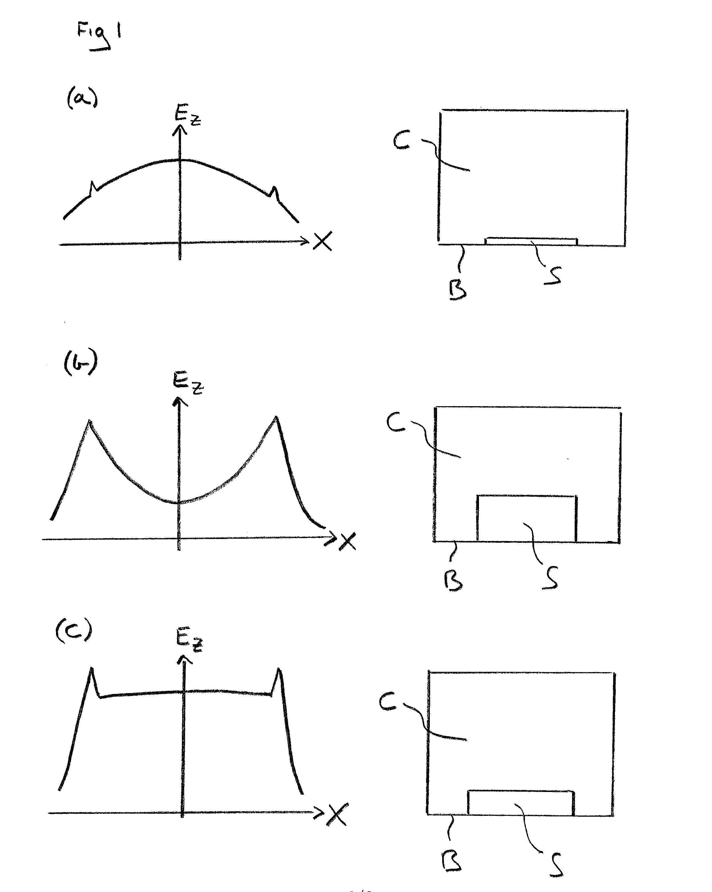
[0061]It is considered desirable to provide a microwave plasma reactor which is configured to form a uniform, large area plasma above a substrate in order to provide uniform CVD diamond growth over a large area of the substrate. Intuitively, one would expect that a microwave plasma reactor should be configured to support a uniform electric field above the substrate in order to form such a uniform plasma. The first aspect of the present invention is based on the seemingly counter-intuitive finding that a non-uniform electric field of a particular form can produce a more uniform plasma over a larger area than a corresponding uniform underlying electric field and that this can lead to more uniform CVD diamond growth over larger areas. In particular, the present inventors have found that it is preferable to form an electric field having an axisymmetric Ez profile comprising a substantially flat central portion bound by a ring of higher electric field, the substantially flat central port...


PUM

PropertyMeasurementUnit
Temperatureaaaaaaaaaa
Lengthaaaaaaaaaa
Lengthaaaaaaaaaa

Abstract

A microwave plasma reactor for manufacturing synthetic diamond material via chemical vapour deposition, the microwave plasma reactor comprising: a microwave generator configured to generate microwaves at a frequency f; a plasma chamber comprising a base, a top plate, and a side wall extending from said base to said top plate defining a resonance cavity for supporting a microwave resonance mode between the base and the top plate; a microwave coupling configuration for feeding microwaves from the microwave generator into the plasma chamber; a gas flow system for feeding process gases into the plasma chamber and removing them therefrom; a substrate holder disposed in the plasma chamber and comprising a supporting surface for supporting a substrate; and a substrate disposed on the supporting surface, the substrate having a growth surface on which the synthetic diamond material is to be deposited in use, wherein the substrate dimensions and location within the resonance cavity are selected to generate a localized axisymmetric Ez electric field profile across the growth surface in use, the localized axisymmetric Ez electric field profile comprising a substantially flat central portion bound by a ring of higher electric field, the substantially flat central portion extending over at least 60% of an area of the growth surface of the substrate and having an Ez electric field variation of no more than ±10% of a central Ez electric field strength, the ring of higher electric field being disposed around the central portion and having a peak Ez electric field strength in a range 10% to 50% higher than the central Ez electric field strength.

Description

FIELD OF INVENTION[0001]The present invention relates to a microwave plasma reactor for manufacturing synthetic diamond material using chemical vapour deposition techniques. Certain embodiments relate to substrates for use in a microwave plasma reactor for synthetic diamond manufacture.BACKGROUND OF INVENTION[0002]Chemical vapour deposition (CVD) processes for synthesis of diamond material are now well known in the art. Useful background information relating to the chemical vapour deposition of diamond materials may be found in a special issue of the Journal of Physics: Condensed Matter, Vol. 21, No. 36 (2009) which is dedicated to diamond related technology. For example, the review article by R. S Balmer et al. gives a comprehensive overview of CVD diamond materials, technology and applications (see “Chemical vapour deposition synthetic diamond: materials, technology and applications” J. Phys.: Condensed Matter, Vol. 21, No. 36 (2009) 364221).[0003]Being in the region where diamond...

Claims


Application Information

Patent Timeline
IPC IPC(8): C23C16/27C23C16/52C23C16/511
CPCC23C16/274C23C16/52C23C16/511C23C16/4586C30B25/105C30B29/04C01B32/26H01J37/32192H01J37/32284Y10T428/12993C23C16/27H01J37/32C23C16/56
Inventor DODGE, CARLTON NIGELINGLIS, PAUL NICOLASSCARSBROOK, GEOFFREY ALANMOLLART, TIMOTHY PETERPICKLES, CHARLES SIMON JAMESCOE, STEVEN EDWARDDODSON, JOSEPH MICHAELCULLEN, ALEXANDER LAMBBRANDON, JOHN ROBERTWORT, CHRISTOPHER JOHN HOWARD
Owner ELEMENT SIX LTD
Learn More