Surface treatment method for stainless steel and housing made from the treated stainless steel
- Summary
- Abstract
- Description
- Claims
- Application Information
AI Technical Summary
Benefits of technology
Problems solved by technology
Method used
Image
Examples
example 1
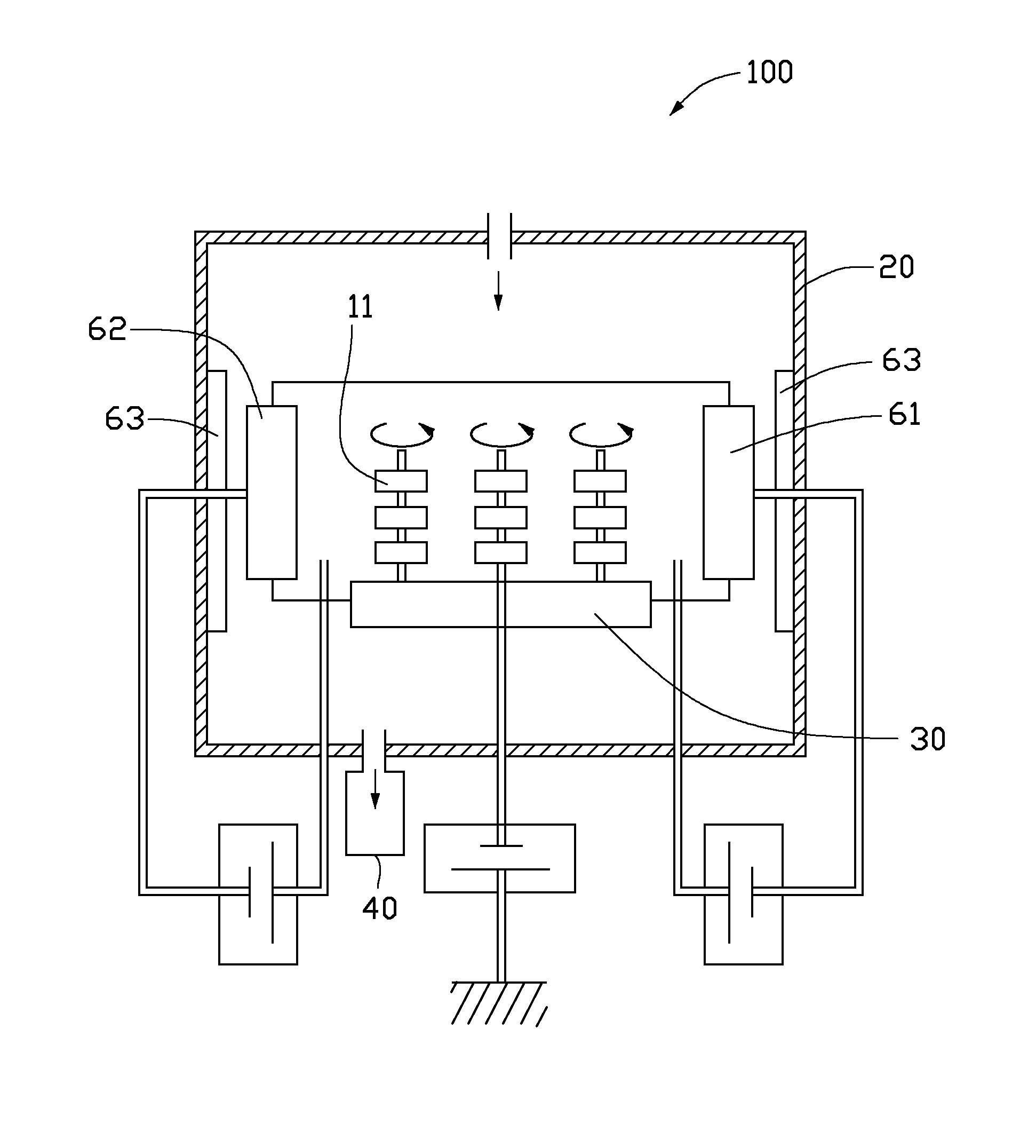
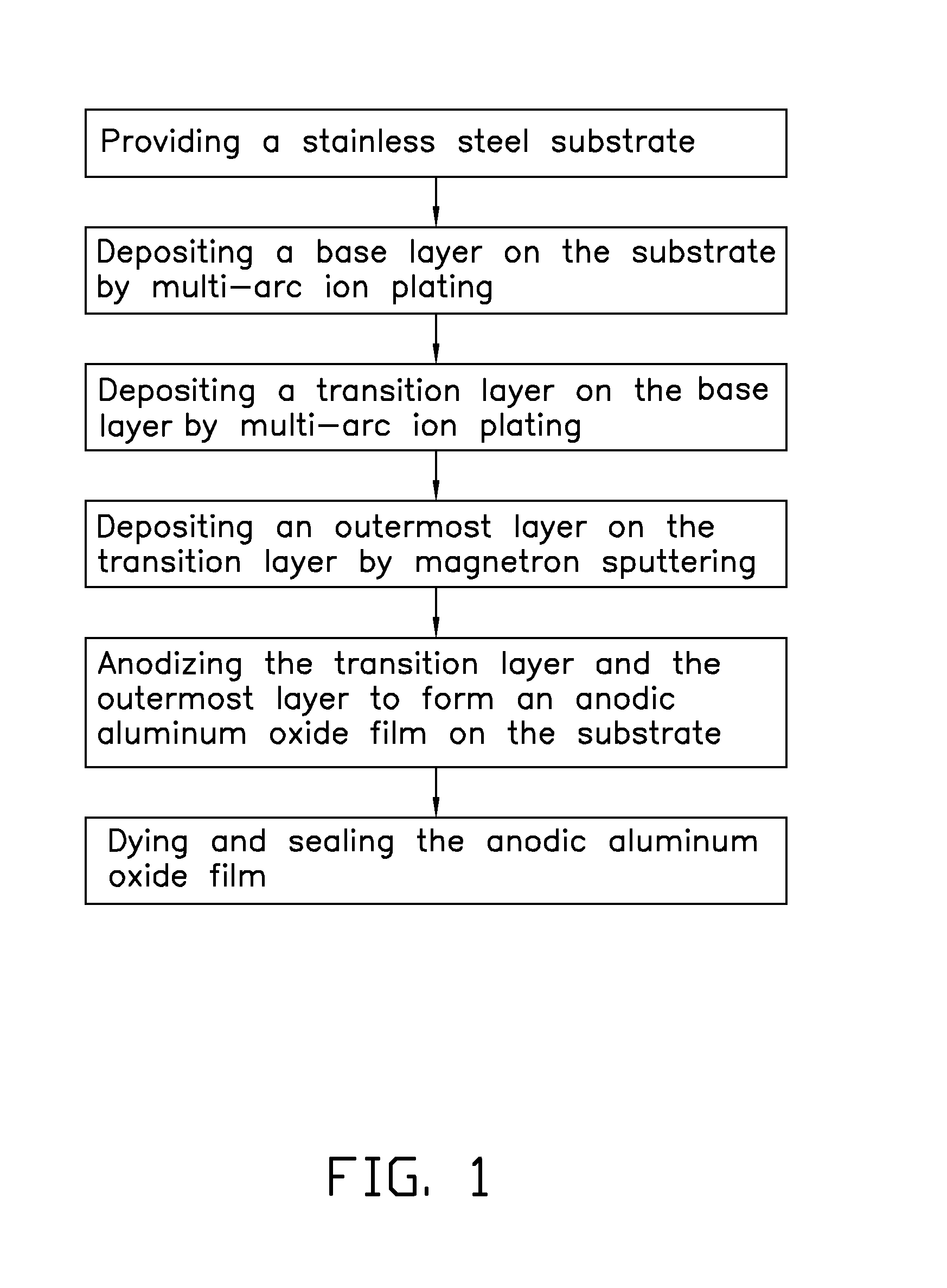
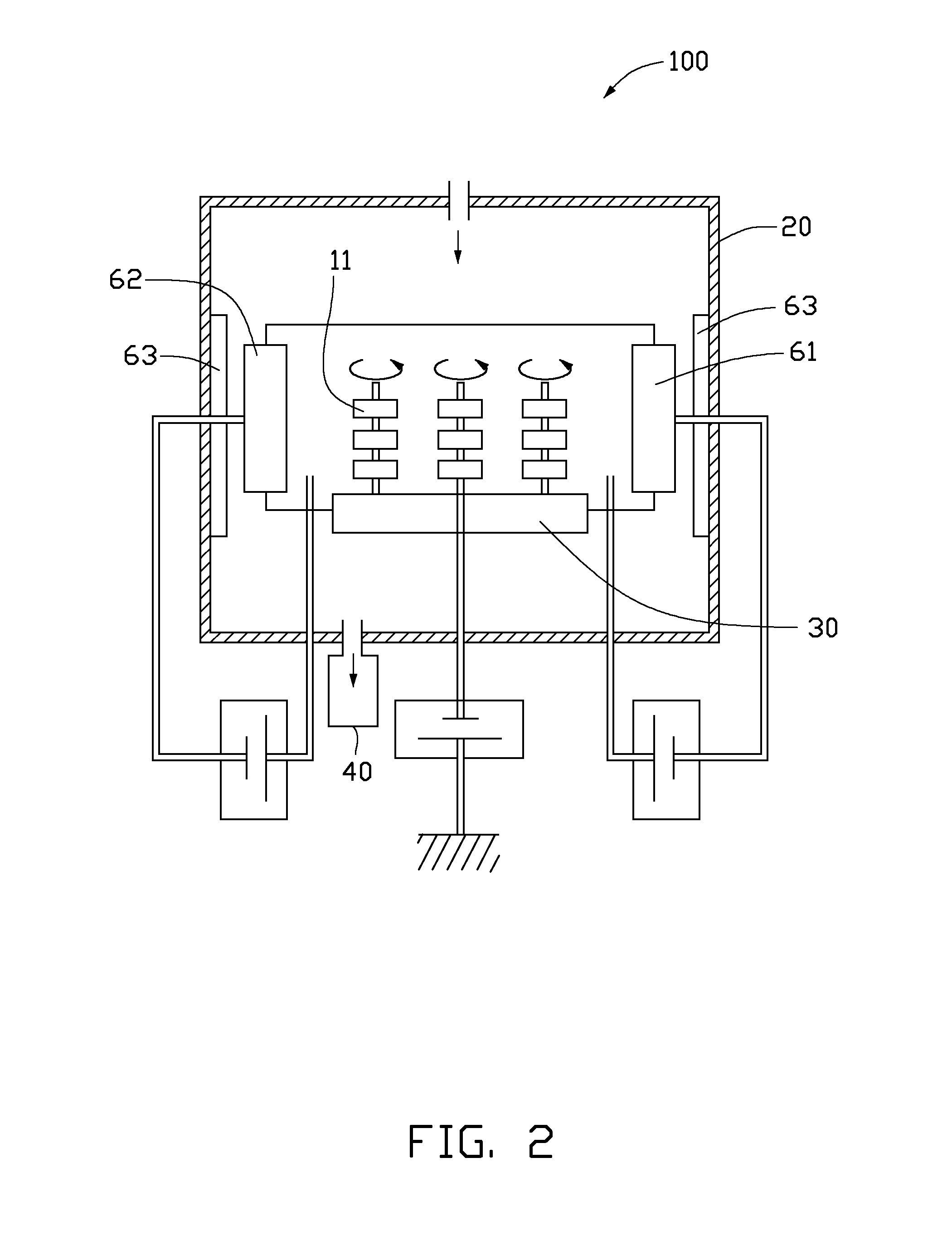
[0026]A base layer 13 was deposited on the substrate 11 by multi-arc ion plating. Eight titanium arc targets 61 were mounted within the chamber 20. The substrate 11 was retained on the rotating bracket 30 in the chamber 20. The chamber 20 was evacuated to about 5.0×10⁻³ Pa. Argon was fed into the chamber 20 at a flow rate of about 100 sccm to adjust the vacuum level inside the chamber 20 to about 0.2 Pa. The temperature in the chamber 20 was set to about 95° C. A bias voltage of about −300 V was applied to the substrate 11. The titanium targets 61 in the chamber 20 were evaporated under an electric power of about 30 V and an electric current of about 75 A. The duty cycle of the electric power was about 50%. Depositing of the base layer 13 took about 10 min. The base layer 13 was a titanium layer having a thickness of about 2 μm.
[0027]A transition layer 15 was deposited on the base layer 13 by multi-arc ion plating. The substrate 11 was retained on the rotating bracket 30 in the cham...
example 2
[0031]A base layer 13 was deposited on the substrate 11 by multi-arc ion plating. The substrate 11 was retained on the rotating bracket 30 in the chamber 20. The chamber 20 was evacuated to about 5.0×10⁻³ Pa. Argon was fed into the chamber 20 at a flow rate of about 80 sccm, to adjust the vacuum level inside the chamber 20 to about 0.15 Pa. The temperature in the chamber 20 was set about 105° C. A bias voltage of about −300 V was applied to the substrate 11. The titanium arc targets 61 in the chamber 20 were evaporated under an electric power of about 20 V and an electric current of about 70 A. The duty cycle of the electric power was about 50%. Depositing of the base layer 13 took about 10 min. The base layer 13 was a titanium layer having a thickness of about 1.5 μm.
[0032]A transition layer 15 was deposited on the base layer 13 by multi-arc ion plating. The substrate 11 was retained on the rotating bracket 30 in the chamber 20. Argon was fed into the chamber 20 at a flow rate of a...
PUM
| Property | Measurement | Unit |
|---|---|---|
| Temperature | aaaaa | aaaaa |
| Temperature | aaaaa | aaaaa |
| Temperature | aaaaa | aaaaa |
Abstract
Description
Claims
Application Information
 - R&D Engineer
- R&D Manager
- IP Professional
- Industry Leading Data Capabilities
- Powerful AI technology
- Patent DNA Extraction
Browse by: Latest US Patents, China's latest patents, Technical Efficacy Thesaurus, Application Domain, Technology Topic, Popular Technical Reports.
© 2024 PatSnap. All rights reserved.Legal|Privacy policy|Modern Slavery Act Transparency Statement|Sitemap|About US| Contact US: help@patsnap.com


