Plasma generation apparatus, CVD apparatus, and plasma-treated particle generation apparatus

a technology of plasma generation apparatus and cvd apparatus, which is applied in the direction of plasma technique, coating, electric discharge lamps, etc., can solve the problems of deterioration in the performance of semiconductor functions, long time required for film formation, and difficulty in considerably improving the time period for film formation, so as to prevent the occurrence of inner surface corrosion, prevent the occurrence of electrode portion corrosion, and reduce the effect of deterioration

Active Publication Date: 2014-05-08
TOSHIBA MITSUBISHI-ELECTRIC IND SYST CORP
View PDF6 Cites 12 Cited by
  • Summary
  • Abstract
  • Description
  • Claims
  • Application Information

AI Technical Summary

Benefits of technology

[0027]The plasma generation apparatus according to the present invention includes: an electrode cell; a power source part configured to apply an AC voltage to the electrode cell; and a housing that encloses the electrode cell. The electrode cell includes: a first electrode; a second electrode facing the first electrode so as to form a discharge space; a dielectric arranged on at least either one of a main surface of the first electrode facing the discharge space and a main surface of the second electrode facing the discharge space; and a pass-through formed in a central portion of the electrode cell in a plan view, the pass-through penetrating the electrode cell with respect to a facing direction in which the first electrode and the second electrode face each other. The plasma generation apparatus further includes: an insulating tube having a cylindrical shape and arranged in the pass-through, the insulating tube including an ejection hole that is formed in a side surface of the cylindrical shape; and a pipe passage configured to directly supply a source gas from the outside of the housing to the discharge space without being connected to a space within the housing where the electrode cell is not arranged.
[0028]Accordingly, for example, a gas containing an active gas, a metal precursor gas, and fine metal particles can be supplied into each discharge space via the pipe passage without contacting a space within the housing other than the discharge space. This can prevent occurrence of a contact of the active gas with an electrode portion of the electrode cell. Therefore, occurrence of corrosion of the electrode portion, which may be caused by the active gas, is prevented. Since the gas containing the metal precursor gas or the fine metal particles is directly supplied to the discharge space, occurrence of deposition of a metal in a space within the housing other than the discharge space is also prevented.
[0029]The pipe passage is provided that is configured to directly supply the source gas from the outside of the housing to the discharge space without being connected to a space within the housing where the electrode cell is not arranged. A passive film that does not cause corrosion and the like due to a chemical reaction of the active gas, or a platinum film or a gold film that have a high resistance to chemical reaction, is performed on the inner surface of the pipe passage. This can prevent occurrence of corrosion of the inner surface of the pipe passage.
[0030]The source gas containing the active gas, the precursor gas, and the fine metal particles is supplied to generate a plasma excitation gas. Accordingly, in the present invention, a larger amount of plasma excitation gas with a higher concentration can be outputted. The precursor gas is dissociated into metal atoms by means of discharge, and due to an imbalanced discharge chemical reaction of dielectric barrier discharge, the metal atoms obtained as a result of the dissociation and the fine metal particles themselves can be modified into a nitrided material or an oxidized material having a higher function, and outputted.
[0031]In the present invention, the distance for supply from the discharge space where the plasma excitation gas is generated to the hollow portion that outputs the excitation gas is shortest. Additionally, in the present invention, a pressure difference can be caused between the discharge space and the hollow portion of the insulating tube by using a pressure reducer. Accordingly, in the present invention, by using the pressure difference, the plasma excitation gas can be ejected through the ejection hole of the insulating tube by adiabatic expansion, and efficiently led from the discharge space to the hollow portion in which the pressure is reduced. Thus, the present invention is able to suppress occurrence of collision among the plasma excitation gases in a region from the discharge space to the hollow portion, and also can suppress occurrence of collision of the plasma excitation gas with a wall and the like. Therefore, the amount of attenuation caused by collisions of the plasma excitation gas can be suppressed. This enables the plasma excitation gas to be more efficiently guided into the hollow portion.
[0032]In the present invention, the plasma excitation gas is generated by using dielectric barrier discharge that enables injection of discharge energy having a high energy density. It has been revealed that, when dielectric barrier discharge occurs under a state where the discharge space is in a vacuum state in which the pressure is equal to or lower than an absolute pressure 30 kPa, it is difficult to stably obtain discharge plasma having a high energy density, because the gas density is low. In this respect, the present invention adopts a structure in which the pressure difference is generated at the ejection hole of the insulating tube which is located between the discharge space and the hollow portion in a vacuum state in which the pressure is equal to or lower than the absolute pressure 30 kPa. Accordingly, dielectric barrier discharge with a pressure equal to or higher than the absolute pressure 30 kPa, which enables injection of discharge energy having a high energy density, can be performed. Therefore, even when the plasma generation apparatus is made compact, a large amount of plasma excitation gas with a high concentration can be generated.

Problems solved by technology

Therefore, a problem always occurs that the wafer substrate is largely damaged by plasma (ions or electrons) to cause a deterioration in the performance of a semiconductor function.
However, such a film formation process involves a problem that it is difficult to provide a nitrogen radical gas source or an oxygen radical source with a high concentration and a large amount, and consequently a very long time is required for the film formation.
However, this method faces difficulties in considerably improving the time period for film formation.
Moreover, due to the discharge chemical reaction in imbalanced discharge plasma generated by the dielectric barrier discharge, fine particles of a photocatalyst material having a good photocatalyst function is generated.

Method used


Image

  • Plasma generation apparatus, CVD apparatus, and plasma-treated particle generation apparatus
  • Plasma generation apparatus, CVD apparatus, and plasma-treated particle generation apparatus
  • Plasma generation apparatus, CVD apparatus, and plasma-treated particle generation apparatus

Examples


embodiment 1

[0051]In this embodiment, application of a plasma apparatus according to the present invention to CVD (Chemical Vapor Deposition) will be described.

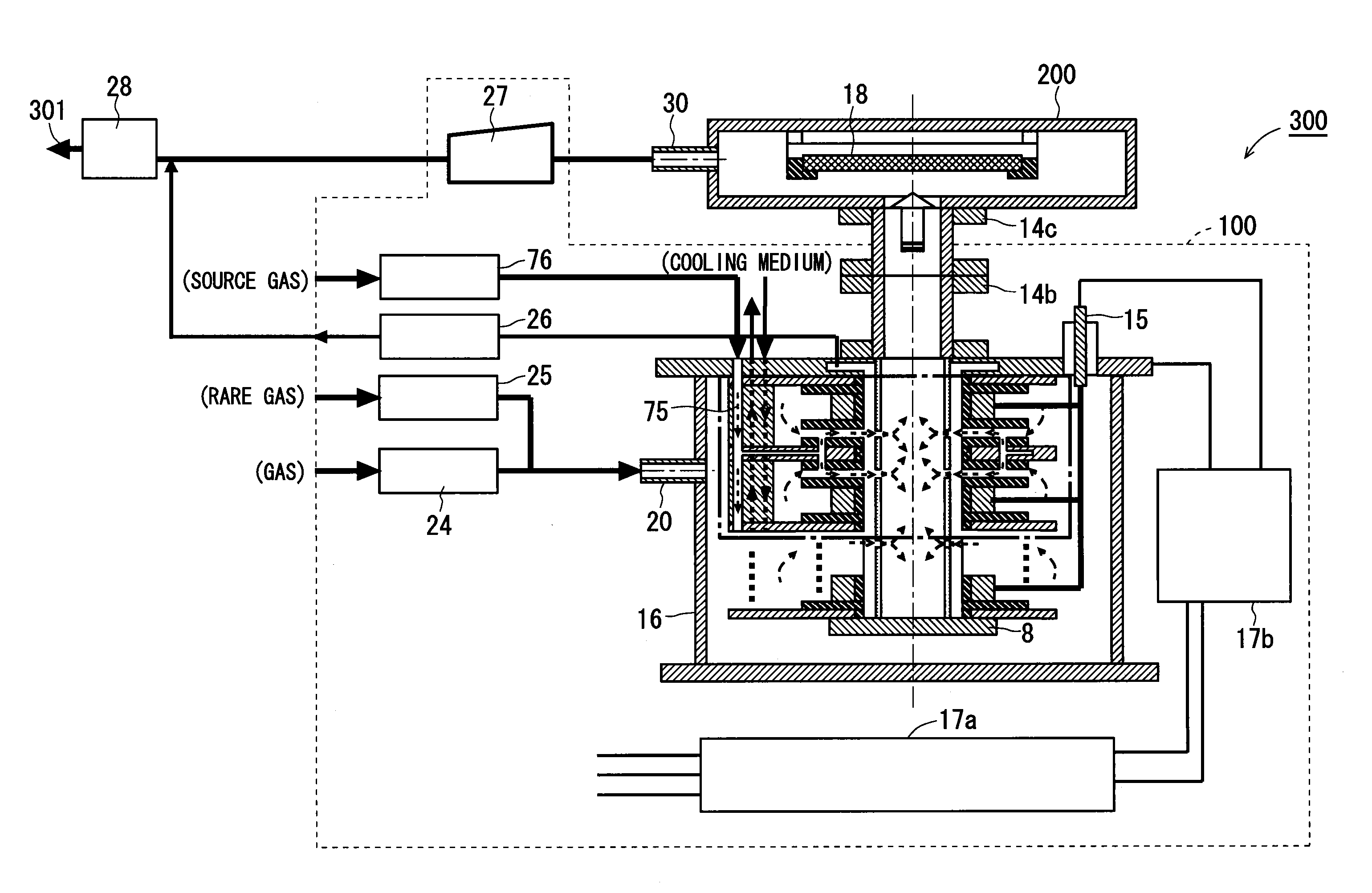
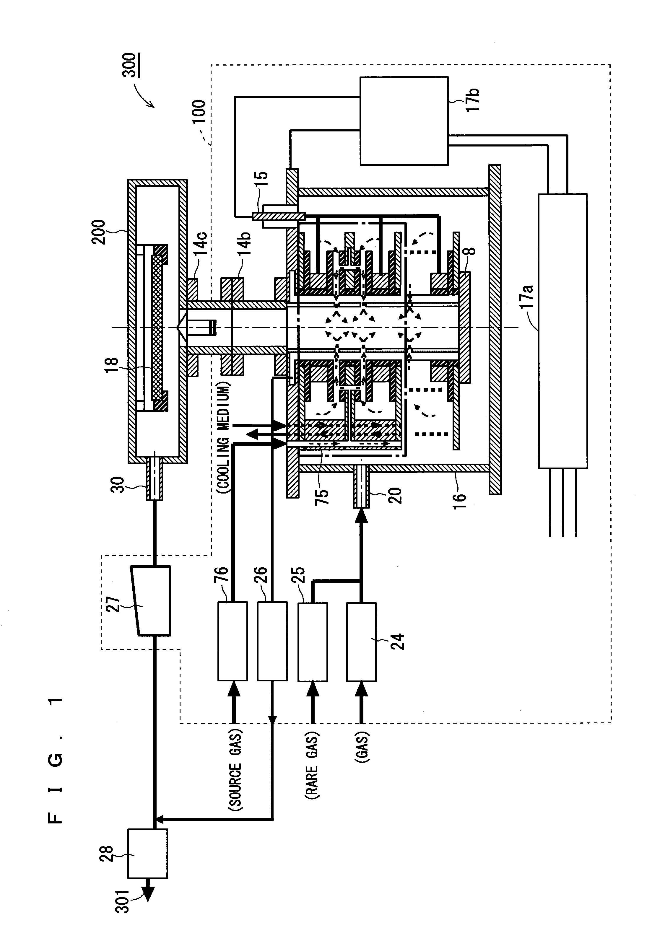
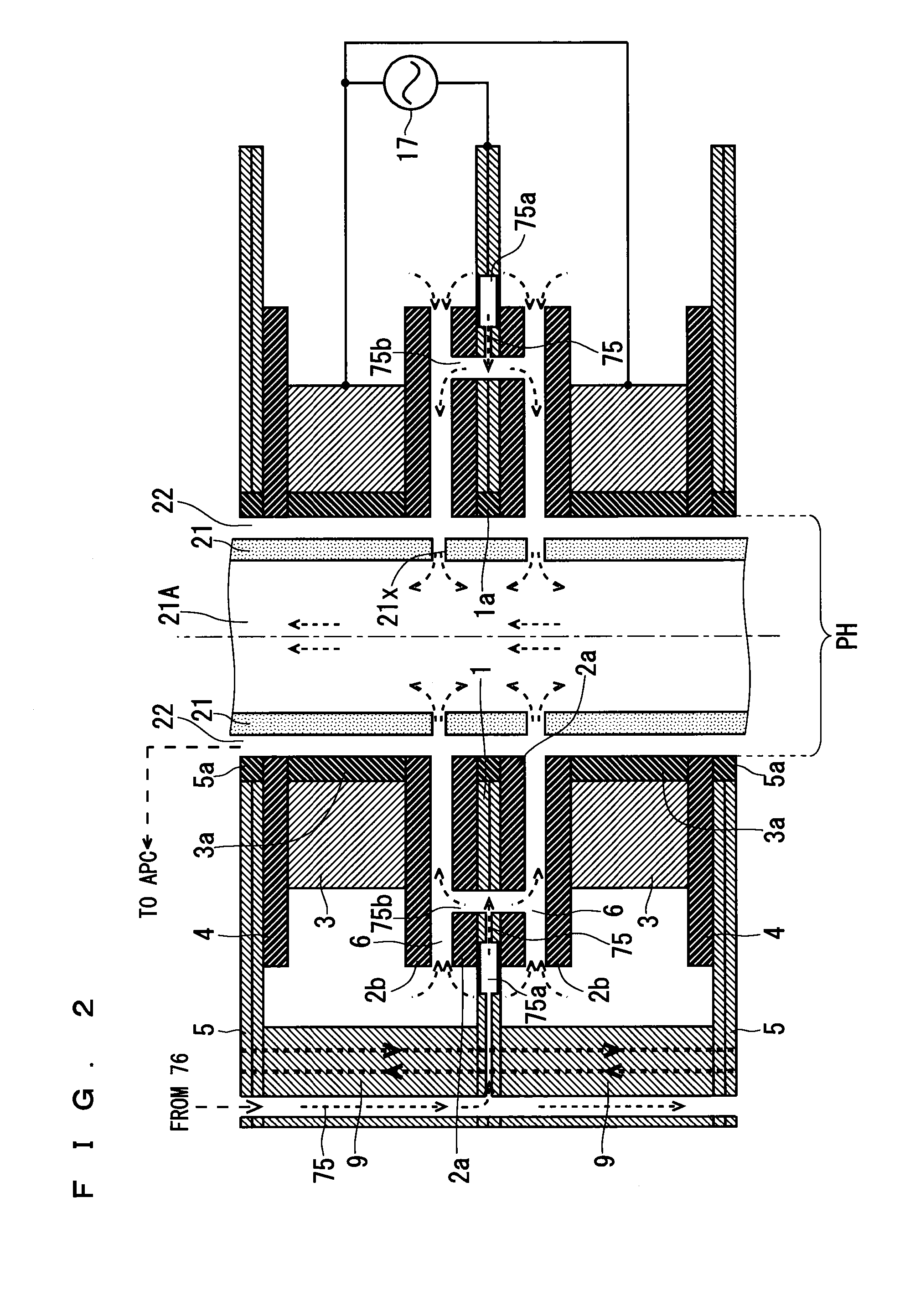
[0052]FIG. 1 is a cross-sectional view showing a configuration of a CVD apparatus 300 according to this embodiment. FIG. 2 is a cross-sectional view showing, on an enlarged scale, a region enclosed by the broken line in FIG. 1 (FIG. 2 discloses a detailed configuration of a cross-section of an electrode cell).

[0053]As shown in FIG. 1, the CVD apparatus 300 includes a plasma generation apparatus 100, a CVD chamber 200, and an exhaust gas decomposition processor 28.

[0054]Firstly, a configuration of the plasma generation apparatus 100 according to the present invention will be described.

[0055]As shown in FIG. 1, in the plasma generation apparatus 100, a plurality of electrode cells are stacked in the vertical direction of FIG. 1. In the cross-sectional view on an enlarged scale shown in FIG. 2, two electrode cells are illustrated. A configu...

embodiment 2

[0154]In this embodiment, application of a plasma apparatus according to the present invention to a plasma-treated particle generation apparatus will be described. The plasma-treated particle generation apparatus is used for an application other than a film formation process in semiconductor manufacturing and the like. For example, a metal material is exposed to discharge plasma in the plasma-treated particle generation apparatus, and thereby the metal material can be modified into new functional material (such as an amorphous material).

[0155]FIG. 4 is a cross-sectional view showing a configuration of a plasma-treated particle generation apparatus 400 according to this embodiment. An electrode cell according to this embodiment has the same configuration as the configuration shown in FIG. 2. In a configuration shown in FIG. 4, unlike the configuration shown in FIG. 1, the auto pressure controller 26 and the pipe passage 22 are not provided.

[0156]The insulating tube 21 shown in FIG. 4...

embodiment 3

[0246]In the plasma discharge apparatus 100 according to the embodiments 1 and 2, the gas containing the active gas and the metal precursor gas or the fine metal particles is directly supplied as the source gas into the discharge space 6 via the pipe passage 75. On the other hand, the inert gas and the rare gas are supplied via the gas supply part 20 to the outer circumferential region of the electrode cell in the housing 16. Thus, the gas containing the active gas and the metal precursor gas or the fine metal particles is prevented from flowing back to a space within the housing 16 other than the discharge space 6.

[0247]As described above, it is necessary to prevent occurrence of the troubles such as corrosion of the electrode within the housing 16, deposition of the metal particles in the discharge space 6 of the housing 16, and the like. From the viewpoint of prevention of the troubles, it is desirable to prevent the gases directly supplied into the discharge space 6 from moving ...


PUM

PropertyMeasurementUnit
energy densityaaaaaaaaaa
pressureaaaaaaaaaa
temperatureaaaaaaaaaa

Abstract

The present invention provides a plasma generation apparatus that, even when a source gas is supplied into a housing where an electrode cell is arranged, does not cause a problem of corrosion of a power feed part and an electrode surface arranged in the housing and a problem of deposition of a metal in a place within the housing other than a discharge part of the electrode cell. A plasma generation apparatus (100) according to the present invention includes an electrode cell and a housing (16) that encloses the electrode cell. The electrode cell includes a first electrode (3), a second electrode (1) facing the first electrode (3) with interposition of a discharge space (6) therebetween, and dielectrics (2a, 2b) arranged on main surfaces of the electrodes (1, 3). The plasma generation apparatus (100) further includes a pipe passage (75) configured to directly supply a source gas from the outside of the housing (16) to the discharge space (6) without being connected to a space within the housing (16) where the electrode cell is not arranged.

Description

TECHNICAL FIELD[0001]The present invention relates to a plasma generation apparatus configured to generate, from a source gas, a large amount of plasma excitation gas (active gas, radical gas) with a high energy and a high concentration, to a CVD apparatus that includes the plasma generation apparatus and that is configured to suppress the amount of attenuation of the generated plasma excitation gas and effectively supply the generated plasma excitation gas to the CVD apparatus, and to a plasma-treated particle generation apparatus including the plasma generation apparatus.BACKGROUND ART[0002]In the manufacture of a semiconductor device, a thermal CVD (Chemical Vapor Deposition) apparatus, a photo CVD apparatus, or a plasma CVD apparatus is used in a method for forming a highly functional film (such as a highly conductive film with a low impedance that corresponds to a circuit wiring in a semiconductor chip, a highly magnetic film having a function as a wiring coil of a circuit or a...

Claims


Application Information

Patent Timeline
Patent Type & Authority Applications(United States)
IPC IPC(8): H01J37/32C23C16/503
CPCC23C16/503H01J37/32449H01J37/32348H05H1/2406C23C16/452C23C16/45557C23C16/45565
Inventor TABATA, YOICHIROWATANABE, KENSUKE
Owner TOSHIBA MITSUBISHI-ELECTRIC IND SYST CORP
Why Eureka
Try Eureka