
Reverse blocking mos semiconductor device and manufacturing method thereof

a reverse blocking and semiconductor technology, applied in semiconductor devices, electrical appliances, transistors, etc., can solve the problems of degrading voltage-withstand reliability, requiring no effective reverse voltage-withstand characteristics, heat deterioration, etc., and reducing reverse leakage currents. the effect of less influence on on-state currents

Inactive Publication Date: 2014-05-01
FUJI ELECTRIC CO LTD
View PDF5 Cites 6 Cited by
  • Summary
  • Abstract
  • Description
  • Claims
  • Application Information

AI Technical Summary

Benefits of technology

The invention provides a method to make a semiconductor device that reduces reverse leakage current and has a small impact on the on-state current. This is helpful in improving the performance of the device.

Problems solved by technology

While, in an ordinary IGBT used for a related electric power conversion circuit, like an ordinary transistor or an ordinary MOSFET having no reverse voltage-withstand characteristic, no effective reverse voltage-withstand characteristic was required.
A large amount of a reverse leakage current is liable to cause heat deterioration to also degrade voltage-withstand reliability.
However, an increase in the amount (dose) of the electron beam irradiation causes degradation in an on state voltage that is in a trade-off relation to the foregoing reduction in a reverse leakage current, increase in a switching speed and enhancement in reverse recovery capability, which imposed limitations to the lifetime control of carriers by the electron beam irradiation.
In particular, in elastic collisions with nuclei, silicon atoms are ejected from their respective lattice sites to form a large number of crystal defects.
However, electron beam irradiation is different from irradiation with other charged particles in that defects are formed in the whole silicon semiconductor substrate when the substrate is irradiated with an electron beam.
As was explained in the foregoing, a reverse blocking IGBT is known to be liable to have a reverse leakage current in a semiconductor substrate increased when a reverse voltage is applied.
Moreover, in the case of a reverse blocking IGBT, it becomes a problem that a reverse leakage current is particularly liable to cause a thermal runaway.
In this way, in a reverse blocking IGBT, an originally large reverse leakage current comes to abruptly increase by a parasitic transistor when a reverse voltage is applied to make the reverse blocking IGBT liable to come to go into thermal runaway.

Method used


Image

  • Reverse blocking mos semiconductor device and manufacturing method thereof
  • Reverse blocking mos semiconductor device and manufacturing method thereof
  • Reverse blocking mos semiconductor device and manufacturing method thereof

Examples


example

[0039]An example of a reverse blocking IGBT and a method of manufacturing thereof will be explained in detail with emphasis on the characterized parts thereof.

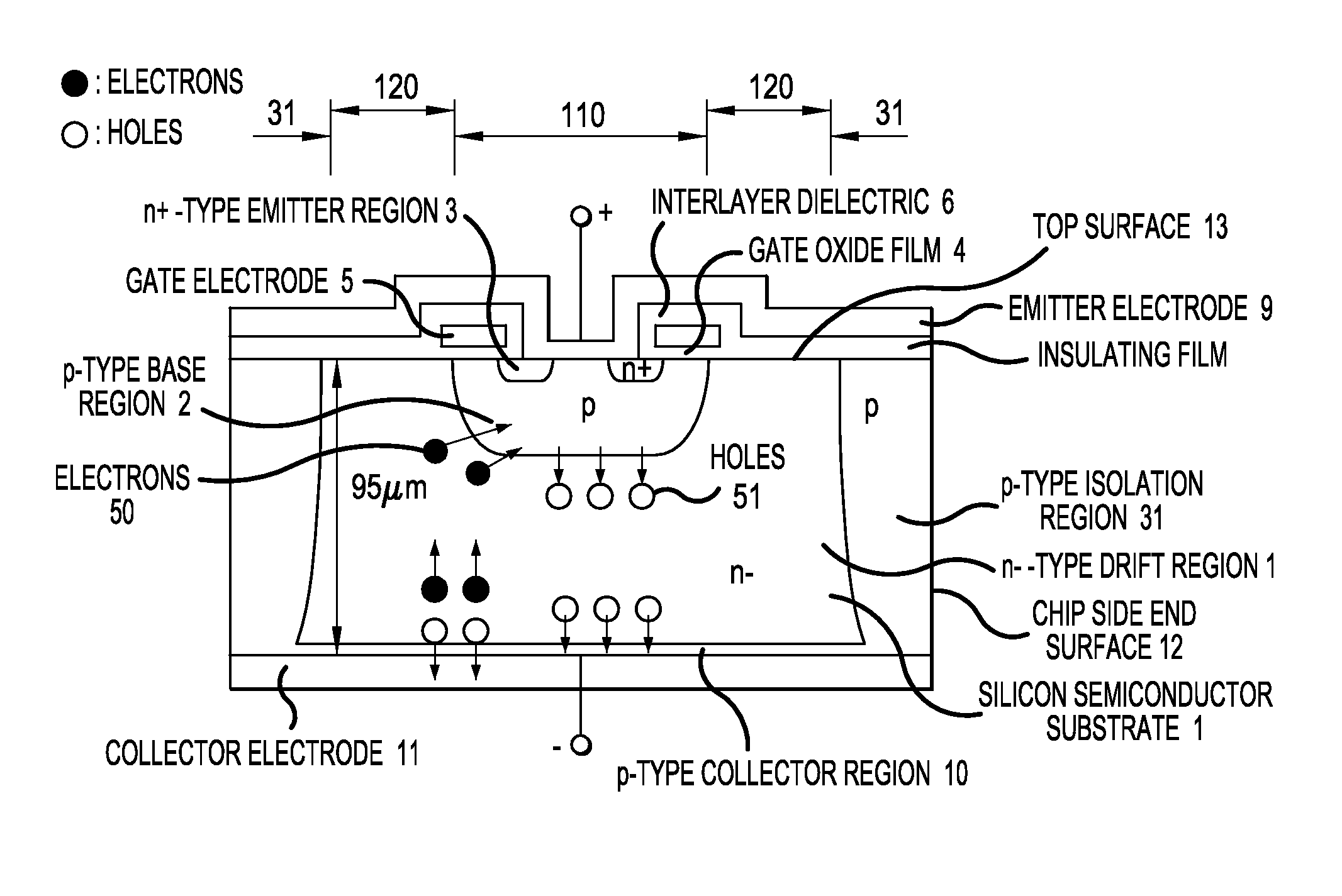
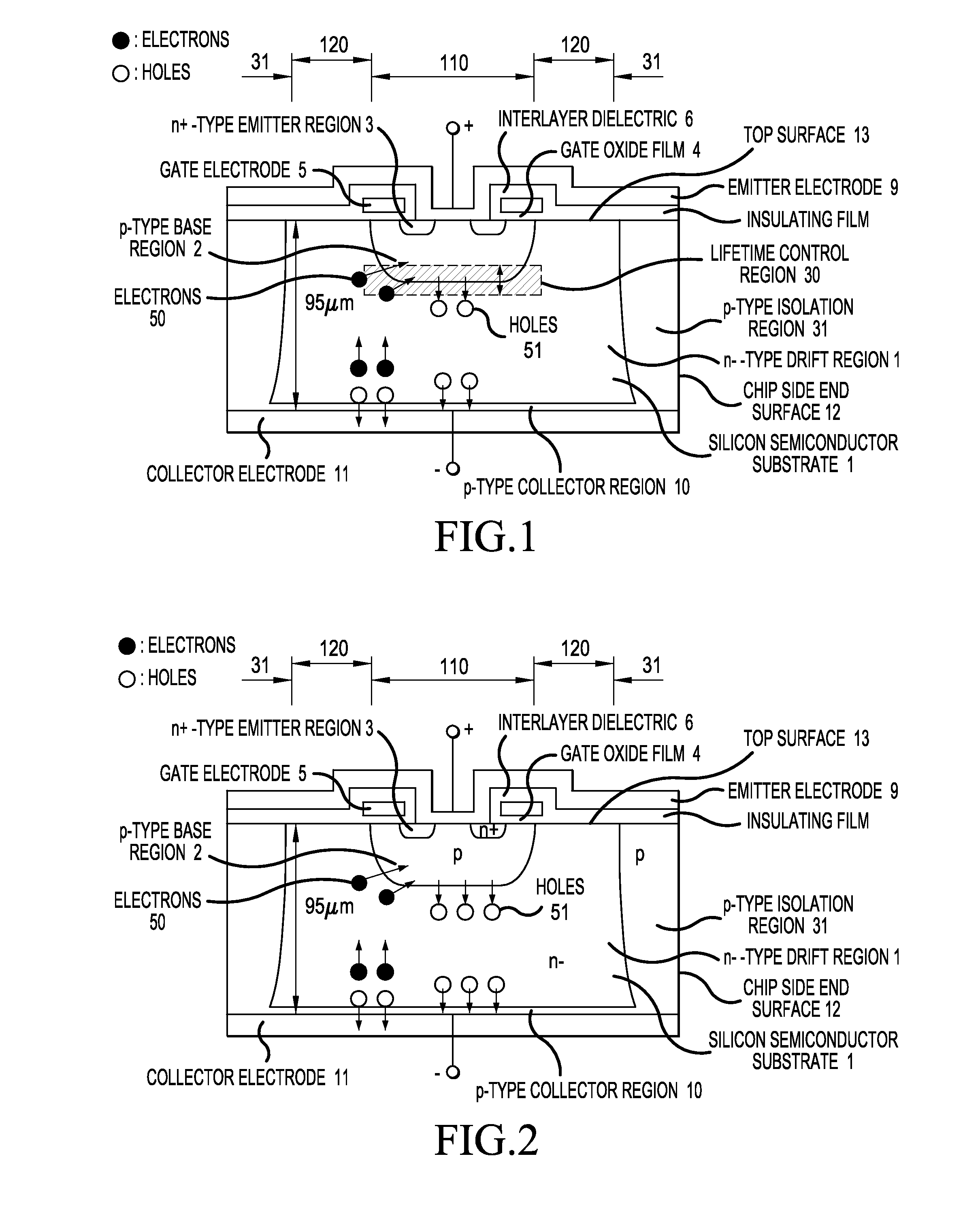
[0040]FIG. 1 is a cross sectional view schematically showing a reverse blocking IGBT with forward and reverse rated breakdown voltages of 600V according to the invention. The reverse blocking IGBT has active region 110 including constituents such as a planar MOS gate structure in the middle section on top surface 13 side of silicon semiconductor substrate 1 of a device chip.

[0041]In a device with a breakdown voltage of 600V, active region 110 is a region becoming the path of the main current of a vertical reverse blocking IGBT. In active region 110, on top surface 13 side of n−-type drift region 1′ with a thickness of 95 μm of silicon semiconductor substrate 1, a MOS gate structure is provided which is formed of p-type base region 2 with a depth of 3 μm, n+-type emitter region 3 with a depth of less than 1 μm, gate oxide film ...


PUM


Abstract

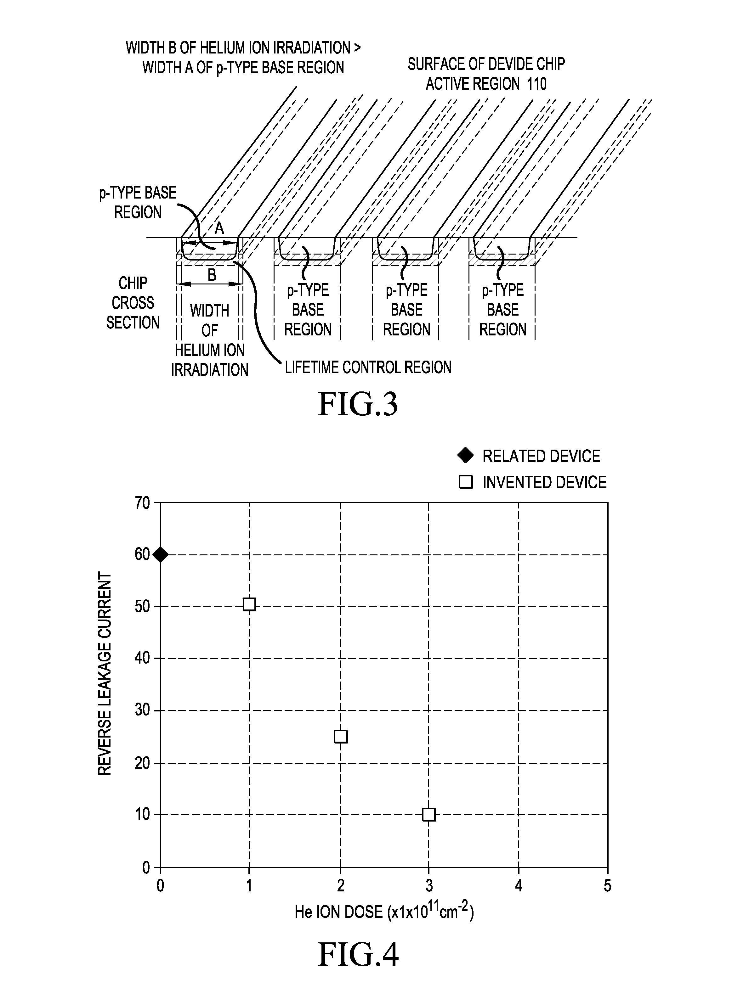
A reverse blocking IGBT is disclosed in which a lifetime control region formed by helium ion irradiation is selectively provided in a region within a range approximately corresponding to the planar pattern of a p-type base region in the direction along the principal surface of a silicon semiconductor substrate of n-type and within a range from the upward vicinity to the downward vicinity of the p-n junction on the bottom of the p-type base region in the direction of the depth of the silicon semiconductor substrate. This can provide a reverse blocking MOS semiconductor device capable of further decreasing a reverse leakage current less than the current in a previous device while making the influence on an on-state current small.

Description

BACKGROUND OF THE INVENTION[0001]A. Field of the Invention[0002]The present invention relates to a reverse blocking MOS semiconductor device such as a reverse blocking IGBT used for a system such as an electric conversion system and a manufacturing method of the device. Here, the term “IGBT” means an insulated gate bipolar transistor.[0003]B. Description of the Related Art[0004]In recent years, in electric power conversion circuits carrying out conversions such as AC (Alternating Current) / AC conversion, AC / DC (Direct Current) conversion, and DC / AC conversion, the use of a matrix converter is known as a directly linked conversion circuit capable of necessitating no DC smoothing circuit formed of components such as electrolytic capacitors and DC reactors. The matrix converter is used under an AC voltage to therefore necessitate bidirectional switching devices, capable of controlling currents in both forward and reverse directions, for a plurality of switching devices mounted on the ma...

Claims


Application Information

Patent Timeline
IPC IPC(8): H01L29/739H01L21/265H01L29/66
CPCH01L29/7393H01L21/265H01L29/66325H01L29/32H01L29/66333H01L29/7395H01L21/263
Inventor KAKEFU, MITSUHIRO
Owner FUJI ELECTRIC CO LTD
Learn More