
Antifuse otp memory cell with performance improvement prevention and operating method of memory

a technology of otp memory cell and performance improvement, applied in the field of memory, can solve problems such as errors in judgment, and achieve the effects of improving performance, preventing yield loss, and improving performan

Active Publication Date: 2014-04-10
EMEMORY TECH INC
View PDF2 Cites 36 Cited by
  • Summary
  • Abstract
  • Description
  • Claims
  • Application Information

AI Technical Summary

Benefits of technology

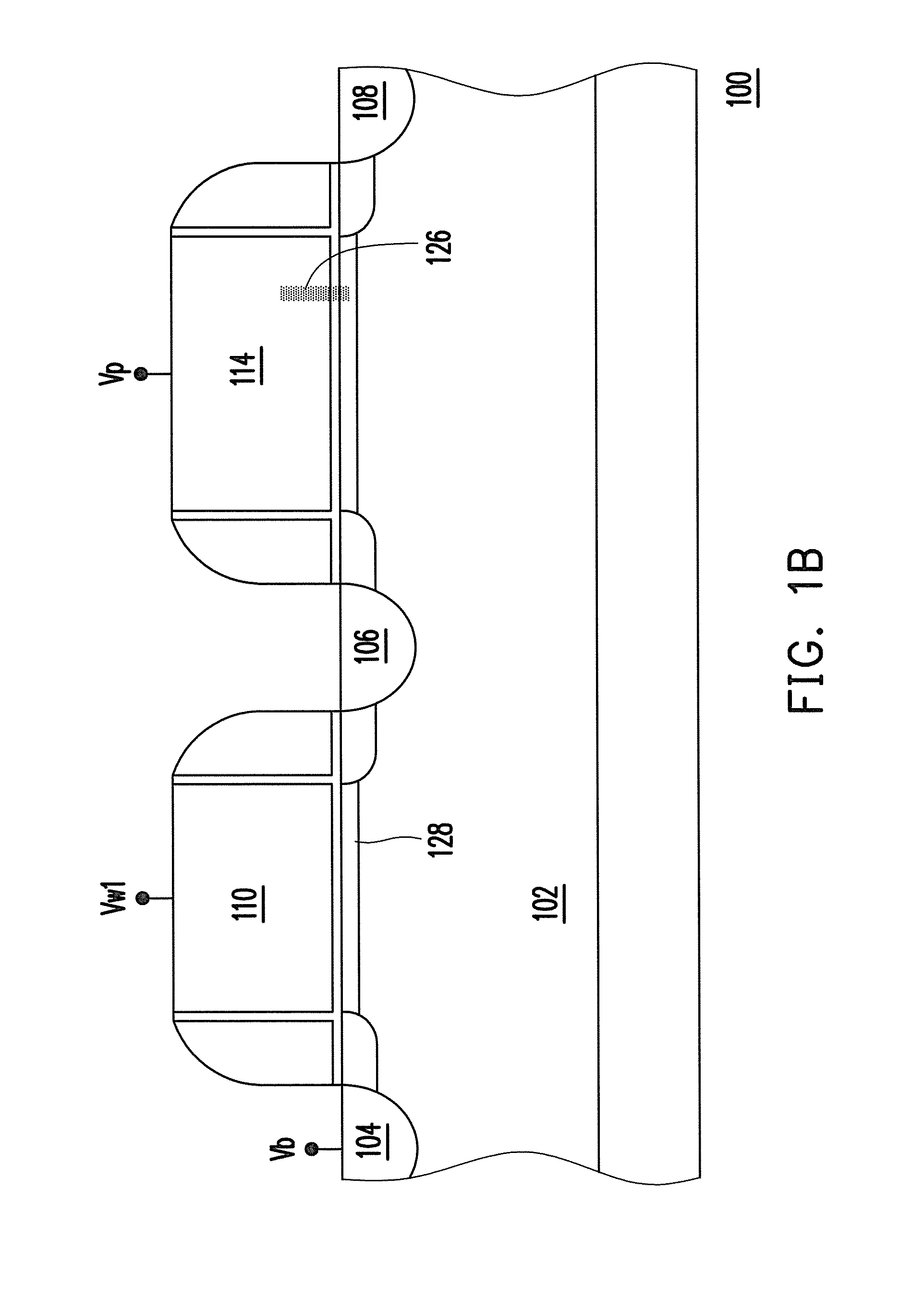
The invention provides an improved antifuse one-time programmable (OTP) memory cell that prevents yield loss caused by a rupture location of an antifuse layer being in a location where an antifuse gate and a substrate are in direct contact. The invention also provides an operating method of a memory that can read using less voltage, lower PGM inhibit current, and reduce gate-induced drain leakage (GIDL) of a select gate. A well region is disposed in a substrate below an antifuse unit and a doapped region is connected through the well region, wherein the conductivity type of each of the well region and the doapped region is the same. Even if the rupture location of the antifuse layer is formed in a location without a doped region, current can still be conducted to the doped region through the well region to prevent the issue of yield loss.

Problems solved by technology

Therefore, operating methods of the OTP memory unit usually result in erroneous judgments due to different forming locations of the conductive path.

Method used


Image

  • Antifuse otp memory cell with performance improvement prevention and operating method of memory
  • Antifuse otp memory cell with performance improvement prevention and operating method of memory
  • Antifuse otp memory cell with performance improvement prevention and operating method of memory

Examples


Embodiment Construction

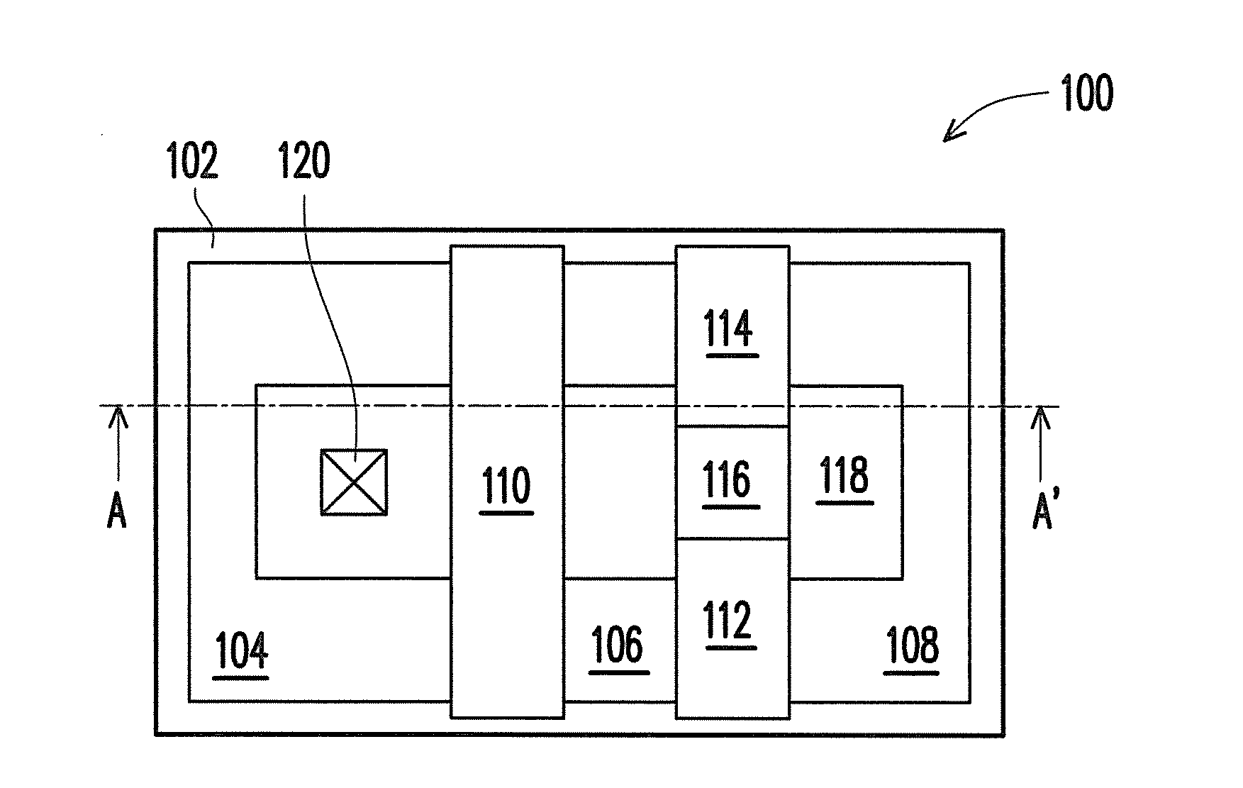
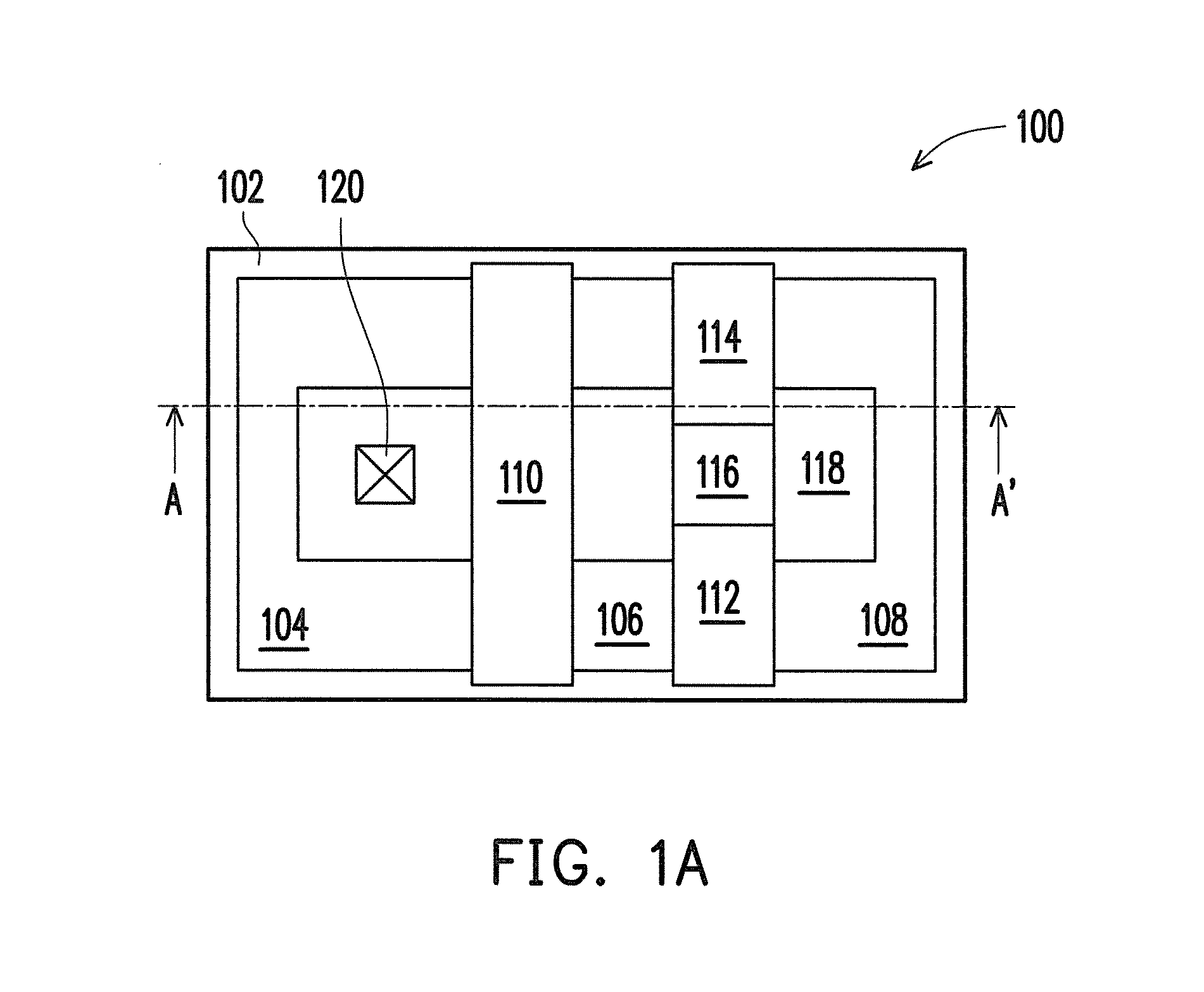
[0042]FIG. 1A is a top view of an antifuse memory cell of an embodiment of the invention. Referring to FIG. 1A, a memory cell 100 includes a well region 102, a select gate 110, a first gate 112, a second gate 114, an insulation layer 116, a first doped region 104, a second doped region 106, a third doped region 108, and a contact plug 120. The well region 102 includes an active area 118. In particular, the insulation layer 116 can be filled between the first gate 112 and the second gate 114.

[0043]In terms of a more complete layout structure, the select gate 110 is fully formed on the active area 118. The first gate 112 and the second gate 114 are respectively partially formed on the active area 118. The first doped region 104 is disposed at a first side of the select gate 110 and the second doped region 106 is disposed at a second side of the select gate 110. From another perspective, the second doped region 106 is disposed at a first side of the first gate 112 and the second gate 1...


PUM


Abstract

Provided is an OTP memory cell including a first antifuse unit, a second antifuse unit, a select transistor, and a well region. The first and the second antifuse unit respectively include an antifuse layer and an antifuse gate disposed on a substrate in sequence. The select transistor includes a select gate, a gate dielectric layer, a first doped region, and a second doped region. The select gate is disposed on the substrate. The gate dielectric layer is disposed between the select gate and the substrate. The first and the second doped region are respectively disposed in the substrate at two sides of the select gate, wherein the second doped region is disposed in the substrate at the periphery of the first and the second antifuse unit. The well region is disposed in the substrate below the first and the second antifuse unit and is connected to the second doped region.

Description

[0001]This application is a continuation-in-part application of and claims the priority benefit of U.S. application Ser. No. 13 / 366,370, filed on Feb. 6, 2012, now allowed. The U.S. application Ser. No. 13 / 366,370 is a continuation-in-part application of and claims the priority benefit of U.S. application Ser. No. 12 / 633,780, filed on Dec. 8, 2009, now U.S. Pat. No. 8,174,063. The U.S. application Ser. No. 12 / 633,780 claims the priority benefit of U.S. provisional application No. 61 / 230,099, filed on Jul. 30, 2009. This application also claims the priority benefit of U.S. provisional application No. 61 / 857,703, filed on Jul. 24, 2013. The entirety of each of the above-mentioned patent applications is hereby incorporated by reference herein and made a part of this specification.BACKGROUND OF THE INVENTION[0002]1. Field of the Invention[0003]The invention relates to a memory and an operating method thereof. More particularly, the invention relates to an antifuse OTP memory cell with p...

Claims


Application Information

Patent Timeline
IPC IPC(8): G11C17/16
CPCH01L29/42344G11C16/10H01L27/11568H01L21/28282H01L29/792G11C17/16G11C17/18H01L23/5252H01L27/11206H01L2924/0002H10B20/25H01L2924/00H10B20/20
Inventor CHEN, CHIN-YICHEN, LUN-CHUNWEN, YUEH-CHIAWU, MENG-YICHEN, HSIN-MING
Owner EMEMORY TECH INC
Learn More