
Multi-band interconnect for inter-chip and intra-chip communications

a multi-band interconnection and communication technology, applied in the field of multi-band rfinterconnect transceivers, can solve the problems of increasing the architectural complexity of the transceiver, requiring a large circuit area, and high overall power consumption

Inactive Publication Date: 2014-02-13
RGT UNIV OF CALIFORNIA
View PDF1 Cites 26 Cited by
  • Summary
  • Abstract
  • Description
  • Claims
  • Application Information

AI Technical Summary

Benefits of technology

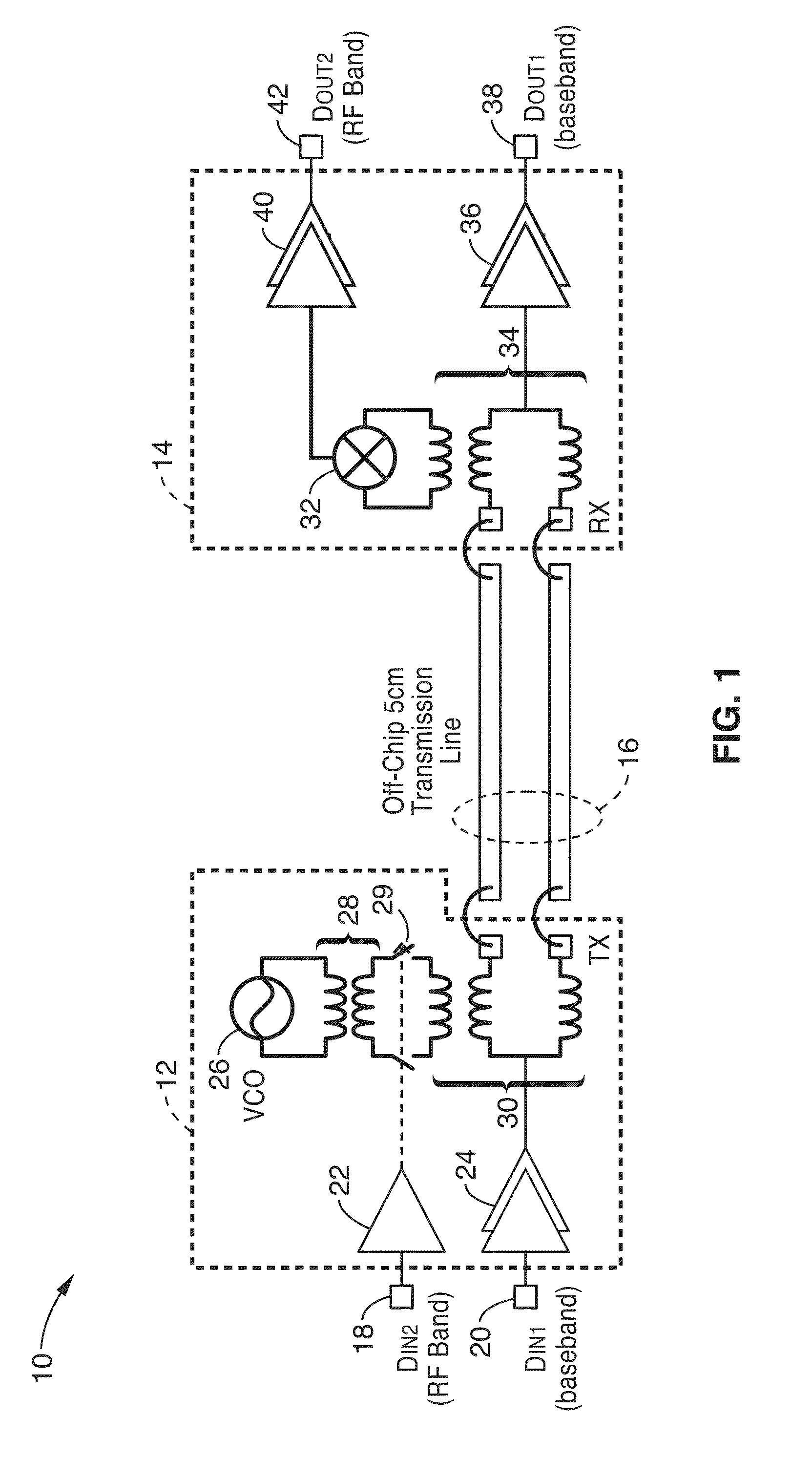
This patent describes a way to send signals between different computer chips simultaneously using a shared transmission line. This allows for faster data transfer and better performance between the chips. The invention can be used in various memory devices and is especially useful for connecting with microprocessors or memory control circuits. Different embodiments of the invention allow for different numbers of channels and directions of transmission. Overall, this patent provides a way to achieve faster and more efficient data transfer between chips.

Problems solved by technology

However, although this interconnection mechanism provides a number of advantages, it suffers from power intensive phase and frequency synchronizations to demodulate binary phase-shift keying (BPSK) at the receiver, which increases transceiver architectural complexity, while requiring a large circuit area and a high overall power consumption.
Consequently, this form of interconnection is not scalable and is not particularly well-suited for use in low power off-chip busses, such as those utilized within parallel memory busses.
However, serial links typically suffer from the need of long initialization time, such as on the order of 1000 clock cycles, and do not meet mobile DRAM I / O requirements for fast switching between active, stand-by, self-refresh and power-down operating modes.
In addition, traditional baseband-only (or BB-only) signaling tends to consume power super-linearly for extended bandwidth due to the need of power intensive pre-emphasis and equalization circuits.

Method used


Image

  • Multi-band interconnect for inter-chip and intra-chip communications
  • Multi-band interconnect for inter-chip and intra-chip communications
  • Multi-band interconnect for inter-chip and intra-chip communications

Examples


embodiment 270

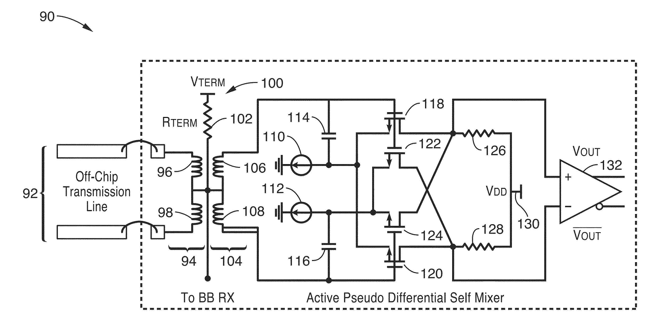
[0095]FIG. 16A through FIG. 16B illustrate an example DBI transceiver embodiment 270 on the DRAM memory side showing an RF-band receiver (RFRX) 272 and a baseband transmitter (BBTX) 274. The RFRX is connected to off-chip transmission line 276 over which it receives the data streams. The data streams are split into the BB and incoming RF-band signal 282 in response to the operation of an on-chip frequency-selective transformer 286, with center taps connecting to a terminating voltage VTERM and coupled to the baseband output driver circuits. The band-pass filtered RF-band data stream is then injected to the receiver differential mutual-mixer composed of a self mixer having bias current sources 288, 290 coupled through DC blocking capacitors 292, 294 to the gates of a self-mixer cross-coupled core comprising transistors 296, 298, 300 and 302, coupled to another stage through resistors 304, 305, 308, 309, capacitors 306, 310 and transistors 312, 314, 316, 318, whose recovered RF band si...

embodiment 430

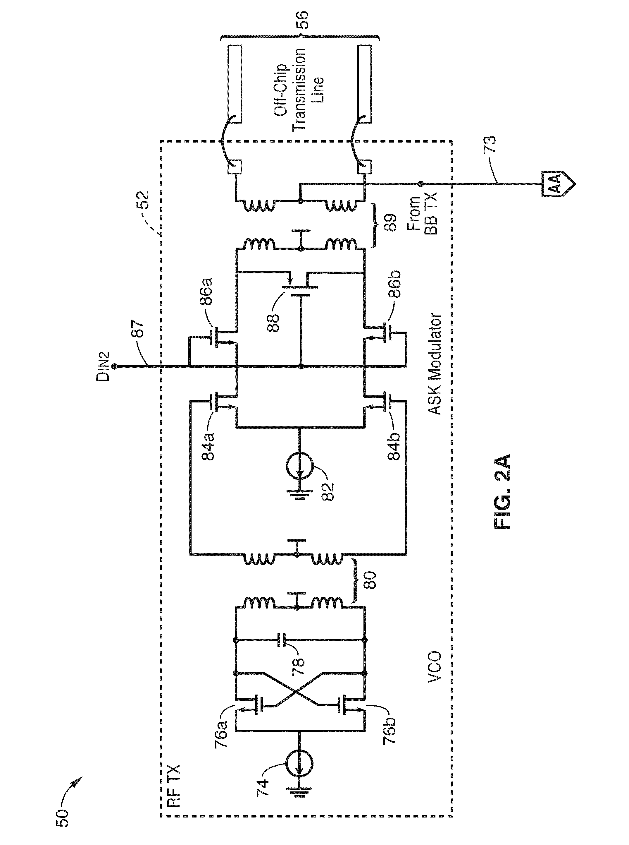
[0124]FIG. 23 illustrates an example MRF-I embodiment 430 as described in prior sections, utilizing one VCO (434a through 434g) per RF transmitter (432a, 432b through 432g) within each of which is shown the ASK TX (436a, 436b through 436g) shown for collectively receiving an RF data input 433, and outputting over multiple differential transmission lines 438.

embodiment 450

[0125]FIG. 24 illustrates an example MRF-I embodiment 450 utilizing one VCO 454 shared for all RF transmitter (452a, 452b through 452g) within each of which is shown the ASK TX (456a, 456b through 456g) shown for collectively receiving an RF data input 453, and outputting over multiple differential transmission lines 458.

[0126]Following is a brief overview of existing DIMM technologies in order to understand the tradeoffs of MRF-DIMM, T-DIMM, and MT-DIMM.

[0127]FIG. 25 depicts a traditional DDRx DIMM consisting of multiple DRAM chips that are accessed in parallel. Simulations were performed assuming each DIMM contains 8 DRAM chips with each chip containing 8 data pins. A 64-bit data bus was formed by aggregating the data signals from each chip. Since the signals were aggregated from each chip to form the 64-bit data bus, each of the 64 data lines is connected to only one of the DRAM chips. However, each command, address, and control signal is connected to every one of the 8 DRAM chip...


PUM


Abstract

Systems, apparatus, modules, and methods of communicating with memory devices utilizing multi-band communication containing a baseband and one or more amplitude shift keyed (ASK) RF channels over each differential pair of off-chip transmission lines. Configurations are described for interfacing between microprocessors, or controllers and memory devices or modules, and within a DIMM and its DRAM devices, and between multiple DIMM memory modules.

Description

CROSS-REFERENCE TO RELATED APPLICATIONS[0001]This application is a 35 U.S.C. §111(a) continuation of PCT international application number PCT / US2012 / 02132 filed on Feb. 14, 2012, incorporated herein by reference in its entirety, which is a nonprovisional of U.S. provisional patent application Ser. No. 61 / 442,557 filed on Feb. 14, 2011, incorporated herein by reference in its entirety, a nonprovisional of U.S. provisional patent application Ser. No. 61 / 443,154 filed on Feb. 15, 2011, incorporated herein by reference in its entirety, and a nonprovisional of U.S. provisional patent application Ser. No. 61 / 53 / 732 filed on Aug. 1, 2011, incorporated herein by reference in its entirety. Priority is claimed to each of the foregoing applications.[0002]The above-referenced PCT international application was published as PCT International Publication No. WO 2012 / 112618 on Aug. 1, 2011, which publication is incorporated herein by reference in its entirety.STATEMENT REGARDING FEDERALLY SPONSORED...

Claims


Application Information

Patent Timeline
Patent Type & Authority Applications(United States)
IPC IPC(8): H04L25/02H04L27/04
CPCH04L27/04H04L25/0274G06F2213/0038G11C5/063G11C7/10G11C7/1057G11C7/1084G06F15/7842H04L45/60H04L27/3483H04L2025/03388
Inventor CHANG, MAU-CHUNGTAM, SAI-WANGBYUN, GYUNG-SUKIM, YANGHYOTHERDSTEERASUKDI, KANITIR, JEREMYREINMAN, GLENNCONG, JINGSHENG
Owner RGT UNIV OF CALIFORNIA
Learn More