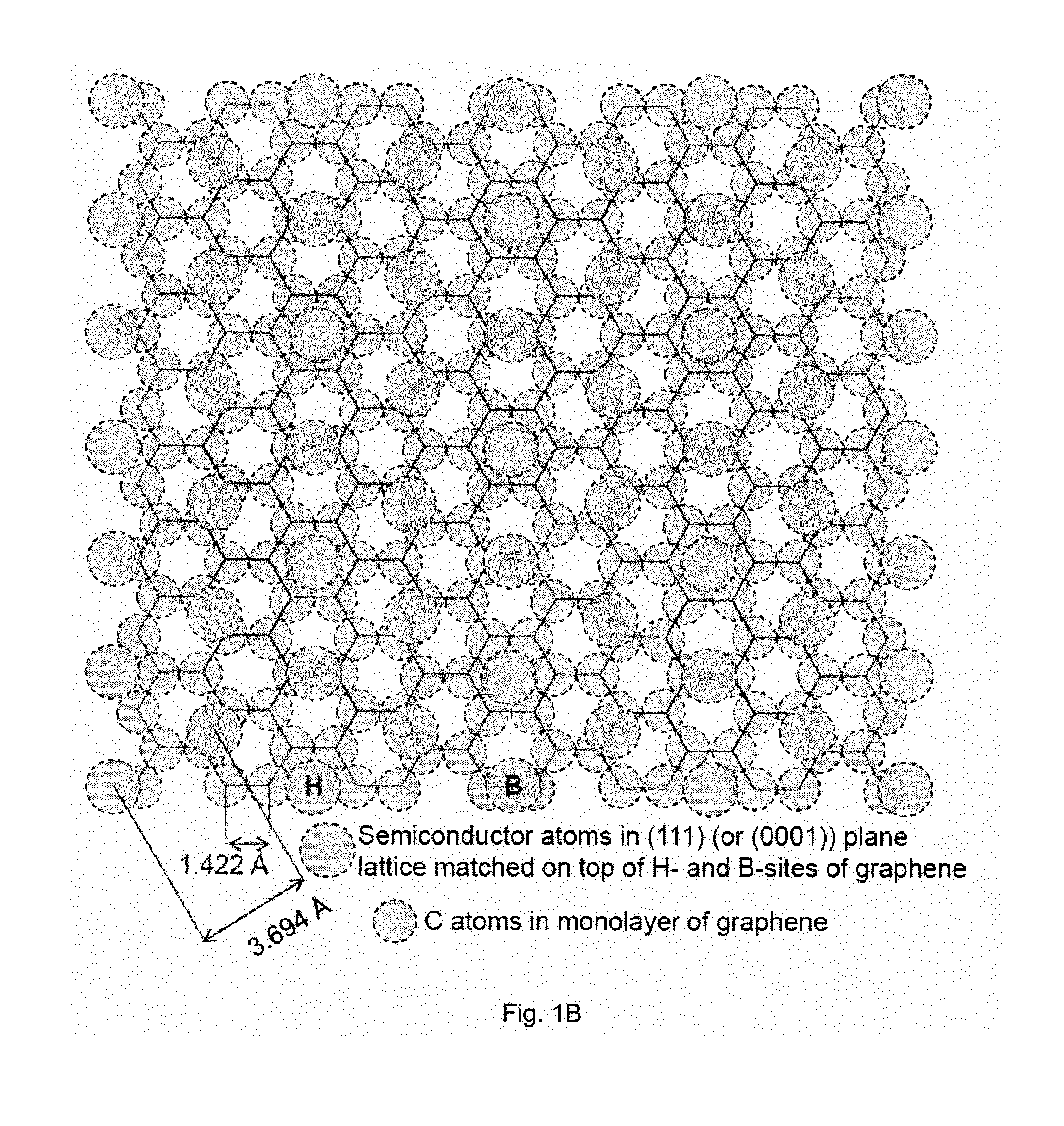
Nanowire epitaxy on a graphitic substrate

a graphitic substrate and nanowire technology, applied in the field of nanowire epitaxy on graphitic substrates, can solve the problems of limiting the growth of nanowires on matching substrates, high cost and limitation, and inability to carry nanowires on gaas substrates, etc., to achieve the effect of enhancing the epitaxial growth of nanowires

Active Publication Date: 2013-12-19
NORWEGIAN UNIVERSITY OF SCIENCE AND TECHNOLOGY (NTNU)
View PDF5 Cites 24 Cited by
  • Summary
  • Abstract
  • Description
  • Claims
  • Application Information

AI Technical Summary

Benefits of technology

The present invention is about growing nanowires on a special type of substrate called graphitic substrates. These substrates are made up of layers of graphene or its derivatives. They are cheap, flexible, and strong, which makes them ideal for growing nanowires. The use of few layered graphene substrates is preferred as they are thin, light, and flexible, but still very strong. The surface of the graphitic substrate can also be chemically or physically modified to enhance the growth of nanowires.

Problems solved by technology

Growing a nanowire on a matching substrate is, however, very expensive and limiting.
For example, GaAs substrates need to be specifically manufactured and that is expensive.
Also, GaAs is not the ideal material to carry a nanowire anyway.
It is not flexible or transparent.
As soon as the substrate is different from the nanowire being grown then there is, by definition, a potential lattice mismatch between substrate and nanowire as well as numerous other possible problems to consider.
Silicon is obviously, a preferred electronics substrate but it too is expensive in pure form.
Moreover, it is not transparent and is not flexible.
It also suffers from a negative interaction with gold, a catalyst often used in nanowire growth.
Plissard et al. concludes, in fact, that the use of gold with a Si substrate is not possible and develops a gold free nanowire growth technique.
However, defect free epitaxial growth of nanowires between such different material classes is not obvious, since (most) semiconductors are three dimensional like with reactive dangling bonds at the surface, whereas graphite has a two dimensional honeycomb structure with no dangling bonds at the surface and thus forms a very inert and hydrophobic surface.
Growing nanowires on substrates such as graphite can also be challenging as large lattice mismatches between the substrate and the growing nanowire were perceived to exist.
Large lattice mismatches can lead to defective nanowires with dislocations or in fact to no nanowire growth at all.

Method used


Image

  • Nanowire epitaxy on a graphitic substrate
  • Nanowire epitaxy on a graphitic substrate
  • Nanowire epitaxy on a graphitic substrate

Examples


example 1

Experimental Procedure

[0130]Nanowires (NWs) were grown in a Varian Gen II Modular molecular beam epitaxy (MBE) system equipped with a Ga dual filament cell, an In SUMO dual filament cell, and an As valved cracker cell, allowing to fix the proportion of dimers and tetramers. In the present study, the major species of arsenic were As4. Growth of NWs is performed either on a Kish graphite flake or on a graphene film (1 to 7 monolayers thick) grown by a chemical vapor deposition (CVD) technique directly on a Ni film deposited on an oxidized silicon wafer. The CVD graphene films were bought from “Graphene Supermarket”, USA. The samples were prepared using two different procedures. In the first procedure, the samples were cleaned by iso-propanol followed by a blow dry with nitrogen, and then In-bonded to the silicon wafer. In the second procedure, a ˜30 nm thick SiO2 layer was deposited in an e-beam evaporator chamber on the samples prepared using the first procedure where after holes of ...


PUM


Abstract

A composition of matter comprising at least one nanowire on a graphitic substrate, said at least one nanowire having been grown epitaxially on said substrate, wherein said nanowire comprises at least one group III-V compound or at least one group II-VI compound or comprises at least one non carbon group (IV) element.

Description

[0001]This invention concerns a process for growing nanowires epitaxially on graphitic substrates. In particular, the invention employs molecular beam epitaxy techniques to grow nanowires epitaxially and ideally vertically on graphitic substrates. The resulting supported nanowires form a further aspect of the invention. The nanowires are preferably semiconductor materials and have wide ranging applications in, for example, the electronics industry or in solar cell applications.[0002]Over recent years, the interest in semiconductor nanowires has intensified as nanotechnology becomes an important engineering discipline. Nanowires, which are also referred to as nanowhiskers, nanorods, nanopillars or nanocolumns etc by some authors, have found important applications in a variety of electrical devices such as sensors, solar cells to LED's.[0003]For the purpose of this application, the term nanowire is to be interpreted as a structure being essentially in one-dimensional form, i.e. is of ...

Claims


Application Information

Patent Timeline
IPC IPC(8): H01L21/02H01L29/06
CPCH01L21/02603H01L29/0676B82Y10/00B82Y30/00B82Y40/00H01L21/02376H01L21/02538H01L21/02551H01L21/02631H01L21/02645H01L21/02653H01L29/1606H01L21/20H01L21/28
Inventor WEMAN, HELGEFIMLAND, BJORN-OVEKIM, DONG CHUL
Owner NORWEGIAN UNIVERSITY OF SCIENCE AND TECHNOLOGY (NTNU)
Why Eureka
Try Eureka