
Memory cell string based on gated-diode cell and memory array using the same

a memory array and diode cell technology, applied in the direction of diodes, digital storage, instruments, etc., can solve the problems of consuming more area and changing the threshold voltage of devices, and achieve the effect of preventing interference of adjacent cells and increasing the degree of integration

Active Publication Date: 2013-12-12
SEOUL NAT UNIV R&DB FOUND
View PDF18 Cites 18 Cited by
  • Summary
  • Abstract
  • Description
  • Claims
  • Application Information

AI Technical Summary

Benefits of technology

The present invention is about a memory cell string that utilizes a gated diode structure to improve integration and reduce the power required for operation. By eliminating certain structures in conventional memory strings and arrays, the invention also increases the degree of integration. The memory cells have a gated diode structure, which separates a wall type semiconductor into two twin fins, and a shielding electrode prevents interference between adjacent cells. Overall, this technology allows for higher efficiency and more efficient memory arrays.

Problems solved by technology

Though the FinFET structure can solve the problems of the above mentioned plane structure, it is always have another problem associated with a high integration because of a limitation in reducing width of a fin needed in one cell and that of oxide / nitride / oxide (ONO) layers formed on the both sides of the fin.
The FET based cell devices oppositely formed to each other interlaying the buried insulating layer have a problem changing threshold voltage of devices due to the interference to each other.
Especially, formation of the pads for contacting to metal interlaying the buried insulating layer with a narrow width causes a design rule matter and so it needs to consume more area.

Method used


Image

  • Memory cell string based on gated-diode cell and memory array using the same
  • Memory cell string based on gated-diode cell and memory array using the same
  • Memory cell string based on gated-diode cell and memory array using the same

Examples


Embodiment Construction

[0043]Detailed descriptions of preferred embodiments of the present invention are provided below with accompanying drawings.

[0044]Embodiment for Nonvolatile Memory Cell String

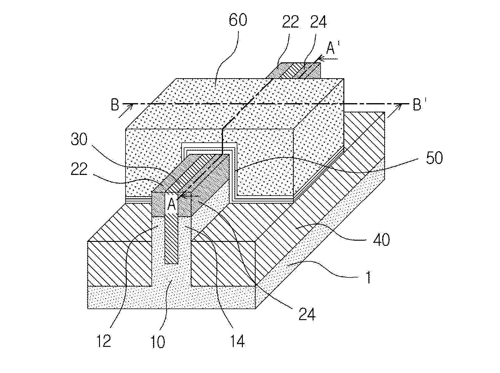
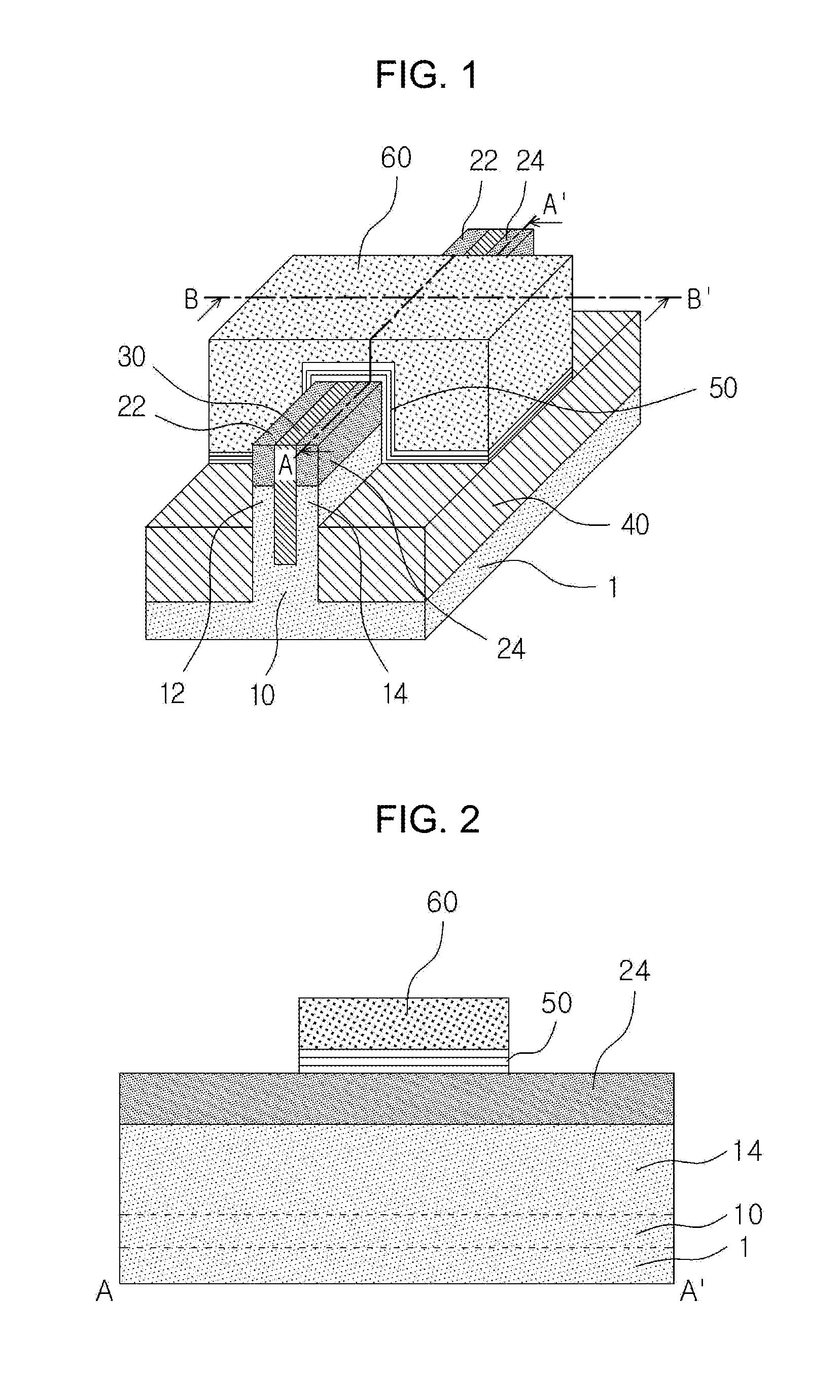
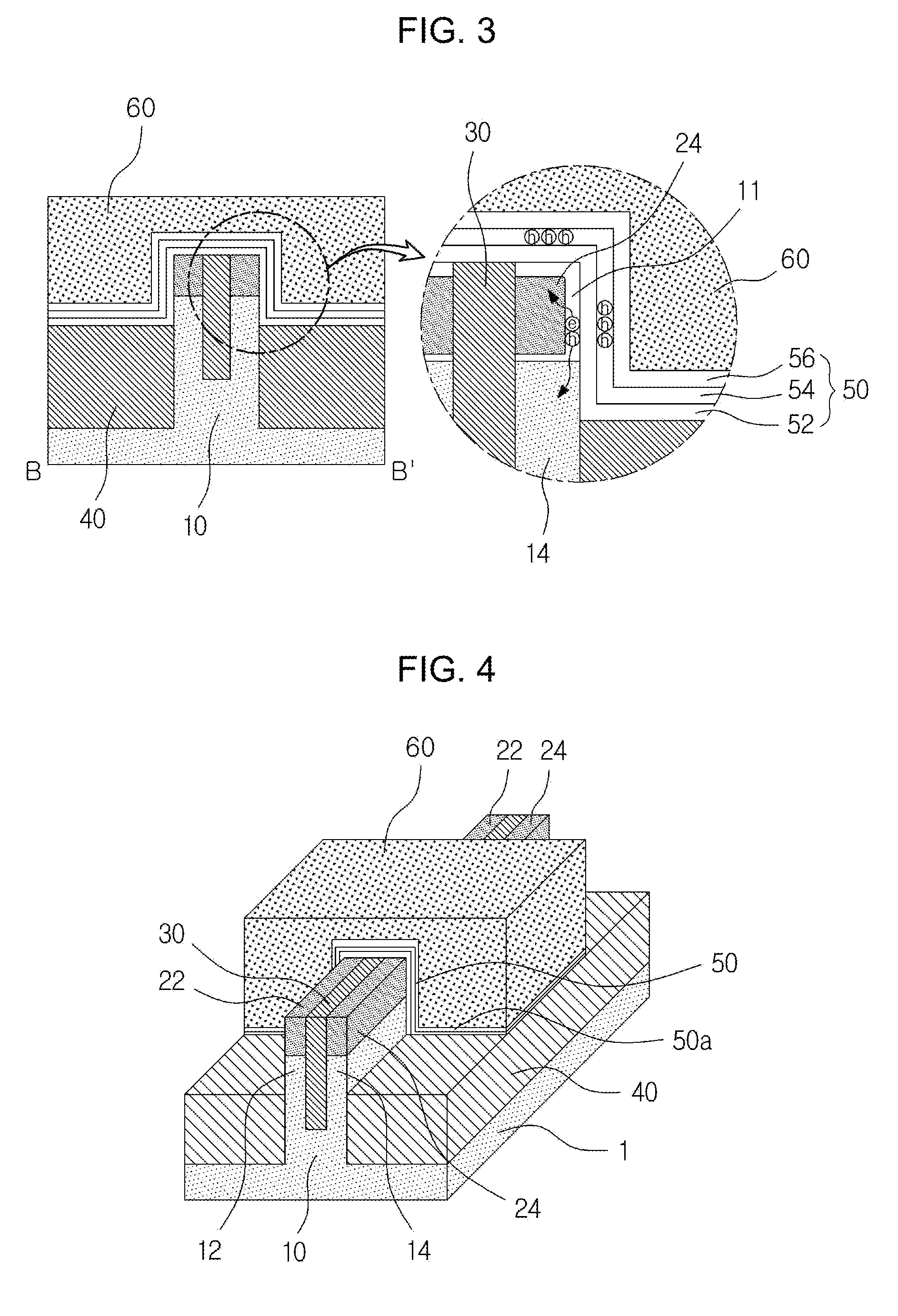
[0045]A nonvolatile memory cell string according to an embodiment of the present invention comprising: two or more cell devices formed in series on a wall type semiconductor protruded from a semiconductor substrate with a predetermined length along one direction to form the cell string, wherein one end of the cell string is electrically connected to outside through one or more string selection transistors formed on one end of the wall type semiconductor, wherein the other end of the cell string is not electrically connected to outside, wherein each of the cell devices is formed to have a gated diode structure on a first semiconductor layer doped with a specific type of impurity on an upper part of the wall type semiconductor and a second semiconductor layer doped with a type of impurity opposite to the first se...


PUM


Abstract

The present invention provides a nonvolatile memory cell string and a memory array using the same. According to the present invention, a wall type semiconductor separated into twin fins and a memory cell string formed with memory cells having a gated diode structure along each fin are enabled to increase the degree of integration and basically prevent the interferences between adjacent cells. And a first semiconductor layer and a depletion region of a PN junction wrapped up by a gate electrode are enabled to remove GSL and CSL by GIDL memory operation and significantly increase the degree of integration for applying to a neuromorphic technology.

Description

CROSS-REFERENCE TO RELATED APPLICATION[0001]This application claims priority under 35 U.S.C. 119 of Korean Patent Application No. 10-2012-0061848 filed on Jun. 9, 2012, the entire contents of which are hereby incorporated by reference.BACKGROUND OF INVENTION[0002]1. Field of the Invention[0003]The present invention relates to a nonvolatile memory cell string and a NAND flash memory array using the same. Additionally, the present invention also relates to neuromorphic technologies mimicking a synapse, a synapse array and functions of neurons and synapses.[0004]2. Description of the Related Art[0005]To increase the degree of integration in a NAND flash memory etc., memory cell devices and structures of memory cell strings thereof connected in series have been continuously studied.[0006]In the recently spotlighted technologies mimicking the functions of neurons and synapses, high integrated memories and strings and arrays connected with the memories are increasingly needed. The functio...

Claims


Application Information

Patent Timeline
Patent Type & Authority Applications(United States)
IPC IPC(8): H01L27/115G11C16/04
CPCH01L27/11563G11C16/0408H01L29/792H01L29/8613H01L29/8615H01L29/8616H01L29/785H10B43/35H10B63/20H10B43/00H01L27/1021
Inventor LEE, JONG-HO
Owner SEOUL NAT UNIV R&DB FOUND
Learn More