Substrate for an organic light-emitting device and method for manufacturing the same

Active Publication Date: 2013-10-31
LG DISPLAY CO LTD
View PDF8 Cites 11 Cited by
  • Summary
  • Abstract
  • Description
  • Claims
  • Application Information

AI Technical Summary

Benefits of technology

The present invention provides a substrate for an organic light emitting diode that has improved light extraction efficiency, is planarized, and is cost-effective. Additionally, it is easy to mass-produce without compromising the performance of the diode.

Problems solved by technology

However, in an operation of passing light generated in the diode through a stacked structure thereof, total reflection occurs, which decreases internal light extraction efficiency of the diode.
However, when an organic material is deposited on the uneven surface, a thickness probably becomes non-uniform, and thus the diode may be electrically unstable.
When wet coating is performed on an uneven surface, in the beginning of the coating, a coated surface is planarized, but as a solvent evaporates, the surface becomes uneven like the coated surface.
Particularly, since a high refractive planarized surface has a low transmission degree and poor mechanical properties of the coating layer, it is increased in loss of light and decreased in physical strength as a thickness of the planarized surface is increased.
As another method, although a method of thickly coating a high refractive inorganic material by deposition and then polishing the resulting layer may be used, it is very disadvantageous in mass-productivity and production cost.
However, the substrate manufactured using the high refractive material is very expensive, and the high refractive substrate is degraded in mechanical properties.

Method used


Image

  • Substrate for an organic light-emitting device and method for manufacturing the same
  • Substrate for an organic light-emitting device and method for manufacturing the same
  • Substrate for an organic light-emitting device and method for manufacturing the same

Examples


example 1

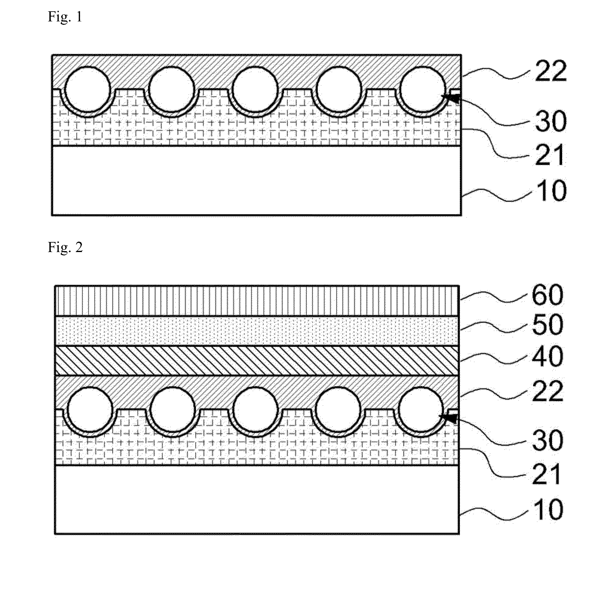
Manufacture of Substrate for Organic Light Emitting Diode

[0057]A coating solution was prepared by sufficiently mixing 1 g of polymer beads (XX75BQ, diameter: 3 μm, Sekisui) having a refractive index of approximately 1.52 in 10 g of a UV curable organic binder (TYT-80-01, solid content: 25 wt %, Toyo ink) in which a high refractive filler is dispersed. Afterward, the coating solution was coated on a surface of a polyester film (PET film) which was not treated with a primer using a coater (#6 Meyer bar coater). Subsequently, the coated coating solution was dried at 100° C. for 2 minutes and cured with an energy of 1 J / cm2 using a UV curing system, thereby manufacturing a film. Separately, a suitable amount of UV curable adhesive (NOA65, Norland Products Inc.) was dropped on a glass substrate for an organic light emitting diode(OLED), the coated coating film was covered such that the coating layer faced the glass substrate, and the polyester film was pressed with a rubber roller to lam...

example 2

[0060]A substrate and an OLED formed on a planarized surface thereof were manufactured by the same method as described in Example 1, except that the number of polymer beads was changed to 1.5 g in preparation of a coating solution.

experimental example 1

Measurement of Roughness

[0063]Degrees of planarization were measured with respect to the substrates manufactured in Examples 1 and 2 and Comparative Examples 1 and 2. Particularly, the maximum height roughness was measured with respect to surfaces of the substrates manufactured in Examples and Comparative Examples, which were opposite to a transparent glass substrate. The maximum height roughness was obtained by measuring a difference between the maximum height and the minimum height of the manufactured sample, which was measured within a 10×10 μm2 region. Measurement results were shown in Table 2.

TABLE 2ComparativeExample 1Example 2Example 1Maximum height0.30.161.4roughness (μm)

[0064]Referring to Table 2, it can be seen that the planarized surfaces of the substrates in Examples 1 and 2 according to an exemplary embodiment of the present invention have a maximum height roughness of within 1 μm, but that in Comparative Example 2 is considerably increased in maximum height roughness. ...


PUM

PropertyMeasurementUnit
Diameteraaaaaaaaaa
Diameteraaaaaaaaaa
Shapeaaaaaaaaaa

Abstract

Provided is a substrate for an organic light emitting diode including a base substrate, a high refractive scattering layer formed on the base substrate, and having a scattering particle scattering light in a high refractive material, and an adhesive layer formed between the base substrate and the high refractive scattering layer to laminate the base substrate with the high refractive scattering layer, wherein the high refractive scattering layer has a structure in which the scattering particle is immersed in the high refractive material, an average thickness of the high refractive scattering layer is smaller than an average diameter of the scattering particle, a surface of the high refractive scattering layer laminated with the base substrate by the adhesive layer has unevenness formed by the scattering particle, the opposite surface of the high refractive scattering layer laminated with the base substrate by the adhesive layer has a planarized surface, and a method for manufacturing the same. The substrate may have an excellent degree of planarization and improved light extraction efficiency without degradation in performance of the diode, and low process and material costs and mass-production of the substrate may be easily achieved.

Description

TECHNICAL FIELD [0001]The present invention relates to a substrate for an organic light-emitting device and a method for manufacturing the same.BACKGROUND ART[0002]An organic electric device refers to a diode capable of inducing the flow of charges between an electrode and an organic material using holes and / or electrons. According to an operation principle, the organic electric device may be an electronic device in a type in which exitons formed in an organic material layer are divided into electrons and holes by a photon input from an external light source to a diode, and each of the divided electrons and holes is transferred to a different electrode and used as a current source; or an electronic device in a type which is operated by holes and / or electrons injected to an organic material by applying a voltage or current to at least two electrodes. An example of the organic electric device is an organic light emitting diode (OLED), an organic solar cell, an organic photo conductor ...

Claims


Application Information

Patent Timeline
IPC IPC(8): H01L51/00
CPCH01L51/0024Y02E10/549G02B5/0242G02B5/0278Y02P70/50H10K77/10H10K50/854H10K50/858H10K71/50
Inventor LEE, YEON-KEUNMOON, JAE MINKANG, JOON KOOJOO, MUN KYUMOON, KYOUNG SIKJANG, SEONG SU
Owner LG DISPLAY CO LTD
Why Eureka
Try Eureka