Cell and module processing of semiconductor wafers for back-contacted solar photovoltaic module
a solar photovoltaic module and semiconductor technology, applied in semiconductor/solid-state device manufacturing, semiconductor devices, electrical equipment, etc., can solve the problem of low photovoltaic efficiency of solar cells as compared to wafers
- Summary
- Abstract
- Description
- Claims
- Application Information
AI Technical Summary
Benefits of technology
Problems solved by technology
Method used
Image
Examples
first example embodiment
[0108]The first example embodiment employs a set of M solar cells laid out in a rectangular pattern of k columns and 1 rows, i.e. the number n of solar cells in the module becomes n=k·l. The example embodiment is illustrated with k=l=2, but may have any even number n of cells.
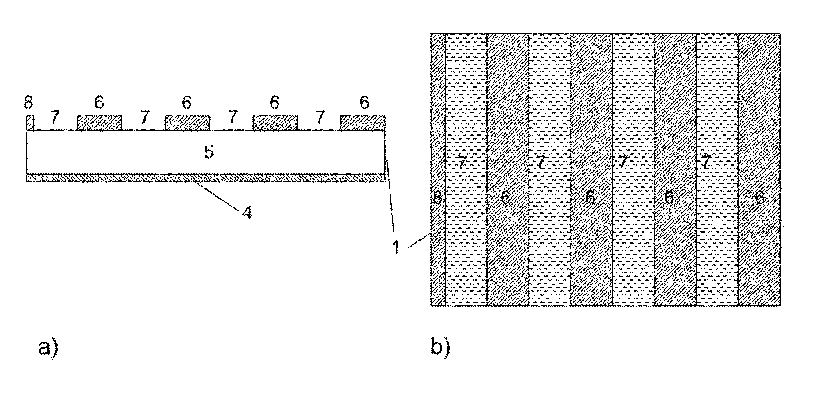
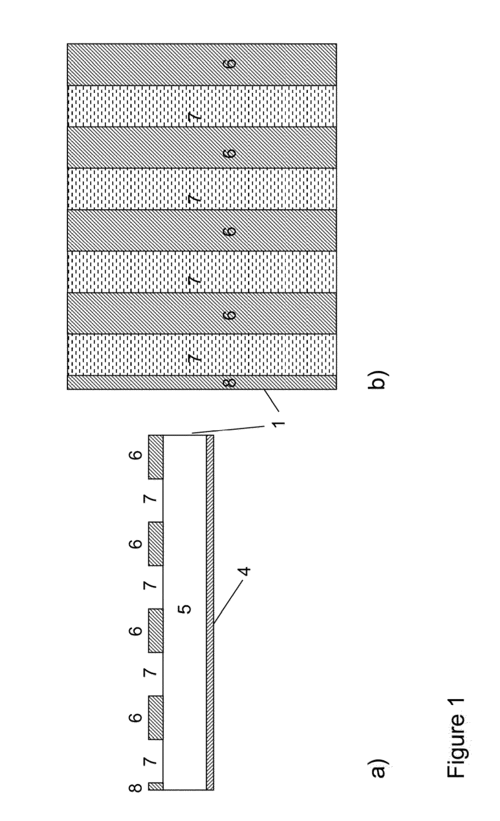
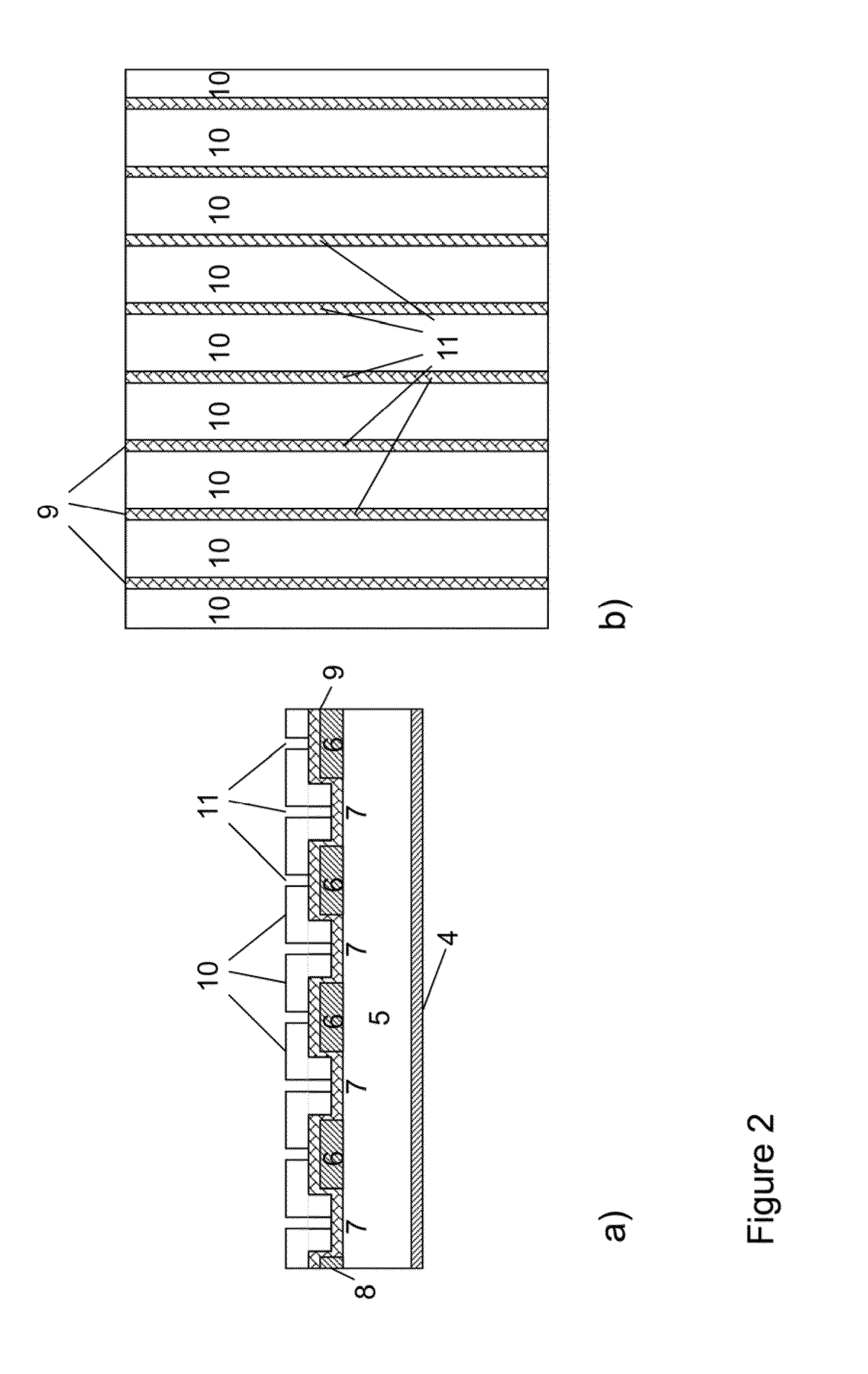
[0109]Each solar cell of the module is made from a quadratic silicon wafer of 125 mm in length and width, and which are laminated onto a front module front glass with a gap or relative distance between their respective side edges of approx. 0.2 mm. Each wafer is made by epitaxial growth of three monocrystalline silicon layers onto a porous release layer of a silicon donor wafer. The first epitaxially deposited layer is the emitter layer and is made to be 0.8 μm thick and doped to a concentration of 1·1019 cm−3 of phosphorous atoms (N-type doping), the second epitaxially deposited layer is the base layer and is made to be 40 μm thick and doped to a concentration of 3·1016 cm−3 of boron atoms (P-type doping), whi...
second example embodiment
[0122]The second example embodiment is a variant of the first example embodiment including the following steps:
1. Texturing the front side followed by diffusion with dopant and formation of an anti-reflection coating to front side of wafer. The front surface is optionally diffused or implanted to form a front surface field or floating junction. Front and back diffusions may be of the same type to achieve a floating junction at the front of the cell, or different types such that a p-n junction is formed at the back side of the cell and a front surface field is formed at the front of the cell. The resulting structure is shown in FIG. 8a).
2. Selectively removing regions of the rear-surface emitter by either:[0123]2.1 a) Coating back side of wafers with etch resist (for example Novolac resin), or optionally screen printing patterned resin and skip inkjet (FIG. 8b).[0124]b) Patterning resist using basic solution (inkjet print), optionally screen printing basic solution to pattern resist ...
PUM
 Abstract
Description
Claims
Application Information
 - R&D
- Intellectual Property
- Life Sciences
- Materials
- Tech Scout
- Unparalleled Data Quality
- Higher Quality Content
- 60% Fewer Hallucinations
Browse by: Latest US Patents, China's latest patents, Technical Efficacy Thesaurus, Application Domain, Technology Topic, Popular Technical Reports.
© 2025 PatSnap. All rights reserved.Legal|Privacy policy|Modern Slavery Act Transparency Statement|Sitemap|About US| Contact US: help@patsnap.com


