Back junction back contact solar cell module and method of manufacturing the same
a solar cell module and back junction technology, applied in the field of back junction back contact solar cell modules and method of manufacturing the same, can solve the problem of low photovoltaic efficiency of solar cells as compared to wafers
- Summary
- Abstract
- Description
- Claims
- Application Information
AI Technical Summary
Benefits of technology
Problems solved by technology
Method used
Image
Examples
first example embodiment
of the Ribbon Geometry
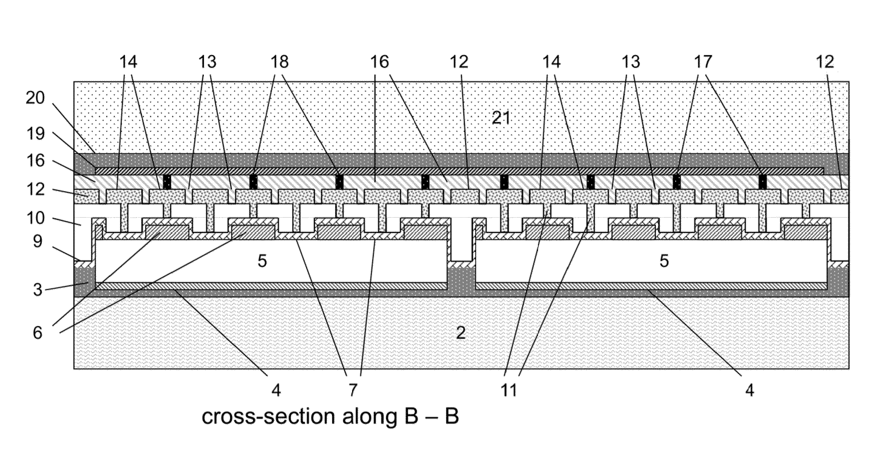
[0121]The first example embodiment of the ribbon geometry is illustrated in FIG. 7a, which in the upper part shows two arbitrarily chosen solar cells 1 number n and n+1 in one row of the solar module. For the cause of clarity the other solar cells 1 in this row (nor in the other rows) are not shown on the figure, and all details related to the solar module are omitted. The Figure does however indicate the underlying finger conductors 14 of the solar cells by the rectangles drawn with a dotted line, and the access openings 17, 18 are shown as dark squares.
[0122]The ribbons 20, 21 of this example embodiment are all rectangular with a constant cross-section and made to span across two sideways adjacent cells in the row, with an exception for the ribbons obtaining contact with either the emitter regions or the base regions of the first or last solar cell in each row. These ribbons will only span one cell. The figure illustrates the span across two cells by showing ...
second example embodiment
of the Ribbon Geometry
[0126]The second example embodiment of the ribbon geometry is illustrated in FIG. 8, and is similar to the first example embodiment except for employing a discontinuous second insulation layer 16 and forming the access openings 17, 18 areas not covered by the second insulation layer.
[0127]The discontinuous second insulation layer is formed by screen printing rectangular areas of the insulation layer in a pattern as shown in the lower part of FIG. 8. The access openings 17, 18 are then located between adjacent rectangular sections of the insulation layer 16 as shown in the upper part of FIG. 8. The formation technique is the same as in the first example embodiment.
PUM
 Abstract
Description
Claims
Application Information
 - R&D
- Intellectual Property
- Life Sciences
- Materials
- Tech Scout
- Unparalleled Data Quality
- Higher Quality Content
- 60% Fewer Hallucinations
Browse by: Latest US Patents, China's latest patents, Technical Efficacy Thesaurus, Application Domain, Technology Topic, Popular Technical Reports.
© 2025 PatSnap. All rights reserved.Legal|Privacy policy|Modern Slavery Act Transparency Statement|Sitemap|About US| Contact US: help@patsnap.com


