
Liquid crystal display

Active Publication Date: 2013-09-05
STANLEY ELECTRIC CO LTD
View PDF5 Cites 3 Cited by
  • Summary
  • Abstract
  • Description
  • Claims
  • Application Information

AI Technical Summary

Benefits of technology

The present invention aims to provide a liquid crystal display that can avoid display defects when simplifying the common electrode. This is achieved by using a simplified patterning process of the common electrode and interposing a non-conductive liquid-crystalline resin film between the routing wire and the common electrode to electrically isolate the area and reduce the likelihood of display defects. This allows for the use of a plastic or film substrate and reduces the processing required. Additionally, the invention allows for the use of a flexible substrate and multiplex driving.

Problems solved by technology

This is because, when the routing wires overlap, change in the alignment of the liquid crystal film in such overlapping area, which is normally not required, will occur, and cause a display defect.
Thus, it is possible to relatively easily realize a shockproof display device or a curved display device that is difficult to be realized when a glass substrate is used.
Nevertheless, since the photolithography technique is often used for the patterning of the segment electrode and the common electrode on the upper and lower substrates, this includes numerous processes that considerably damage the substrate; for instance, heating and cooling of the substrate, irradiation of ultraviolet rays, and exposure to acid chemicals and alkali chemicals.
Nevertheless, options of such a plastic substrate and the like that satisfy all of the foregoing conditions are limited, and also disadvantageous in terms of cost.
In addition, since a substrate is disposed between two polarizers on application to a liquid crystal display, the phase difference in the substrate surface needs to be substantially zero, and the options are even more limited.
Nevertheless, if simplification of causing the entire surface of the substrate to be the common electrode is performed, as described above, change in the alignment of the liquid crystal film will occur in the overlapping area of the routing wire connected to the segment electrode, and the common electrode, the change in the alignment being normally not required, thereby causing a display defect.
The spacer that is in the display area as described above will induce the non-uniformity of the alignment in the liquid crystal film during non-application of voltage or during voltage application, and may cause a drop in the display quality of the liquid crystal display.
Accordingly, since the retardation between the liquid crystal film and the compensating plate cannot be canceled out unless a light-shield film is disposed on at least one of the substrates in an area where the spacer is disposed, leakage of light will occur in the area where the spacer is disposed when the liquid crystal display is viewed from the front or viewed from an oblique direction, and cause a drop in the display quality of the liquid crystal display.
Note that, while it is relatively easy to provide a light-shield film in correspondence to a columnar spacer in which the positional arrangement thereof is predetermined, it is difficult to provide a light-shield film in a case of a spherical spacer that is randomly disposed on the substrate surface via the dry spraying method or the like, in accordance with the position thereof.
Nevertheless, with this type of photosensitive resin, since the photosensitivity and patterning performance tend to deteriorate as a result of increasing the film thickness, it is difficult to obtain a columnar space with sufficient light shielding performance if the film thickness is made to be thicker than 2 μm under the existing conditions.
Moreover, since the number of processes will increase as a result of forming a light-shield film, a light-shield film is not being positively used in a black-and-white liquid crystal display, which does not use a color filter, since it will increase costs.

Method used

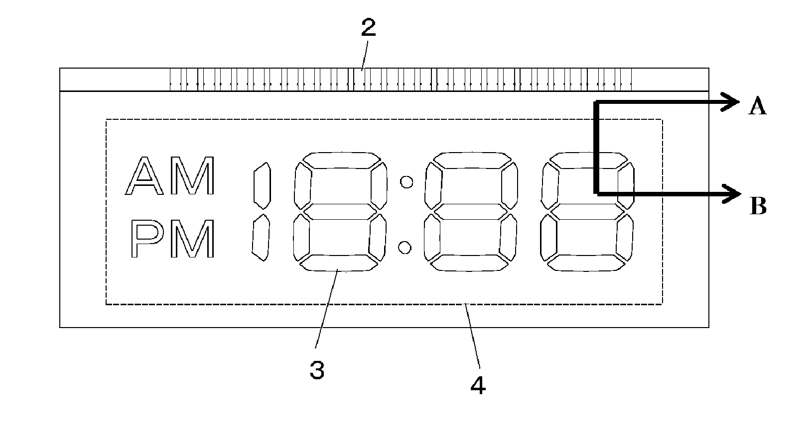
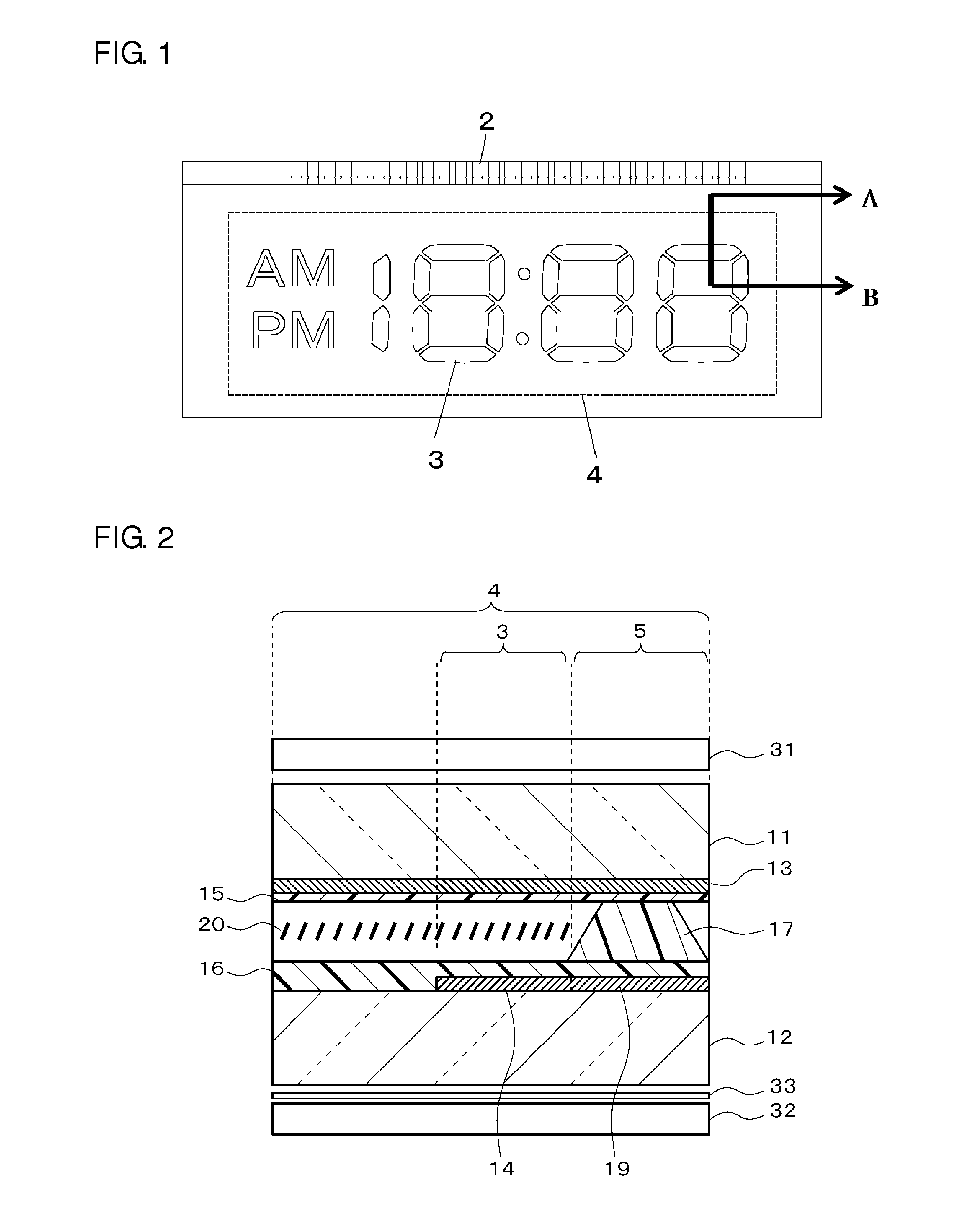
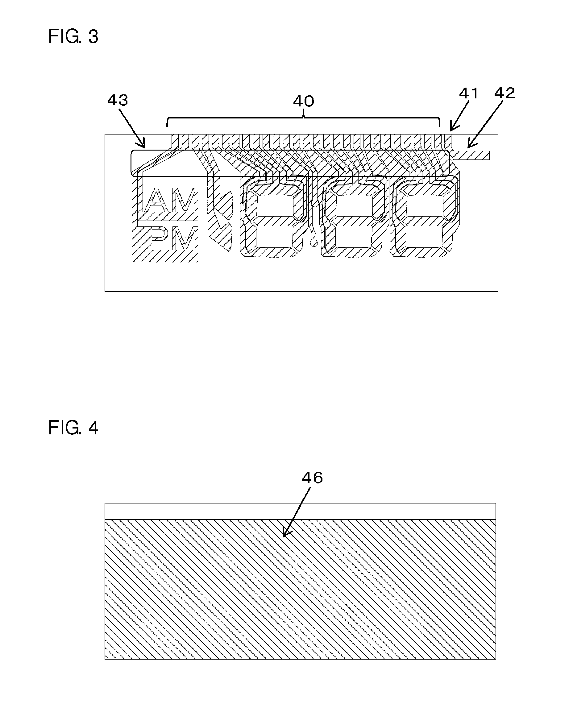

Image

  • Liquid crystal display
  • Liquid crystal display
  • Liquid crystal display

Examples


example 1

[0058]An example of a liquid crystal display in which the upper and lower substrates are glass substrates is now explained.

[0059]Prepared was a substrate having a sheet resistance of 30 n / sq. obtained by one face of a blue plate glass with a thickness of 0.7 mm being polished and subject to a SiO2 undercoat, and a transparent conductive film made of ITO (indium tin oxide) thereafter being deposited on the entire face of the substrate surface. Segment electrodes and routing wires were formed on one face of the substrate by patterning the transparent conductive film via the photolithography process and the wet etching process.

[0060]A vertical alignment film with surface free energy of 35 to 39 mN / m was pattern-printed on this substrate (hereinafter referred to as the “lower substrate”) within the seal frame via the flexographic printing method, tentative calcination was performed at 90° C. for 15 minutes, then main calcination was performed at 180° C. for 30 minutes. Subsequently, bot...

example 2

[0067]An example of a liquid crystal display in which a film substrate is used as the upper substrate, and a glass substrate is used as the lower substrate is now explained.

[0068]An ITO transparent conductive film was deposited, in a thickness of 200 nm, on a white plate glass with a thickness of 0.3 mm by using an in-line sputtering device, and segment electrodes and routing wires were formed on one face of the substrate by patterning the transparent conductive film via the photolithography process and the wet etching process.

[0069]A vertical alignment film with surface free energy of 35 to 39 mN / m was pattern-printed on this substrate (hereinafter referred to as the “lower substrate”) within the seal frame via the flexographic printing method, tentative calcination was performed at 90° C. for 15 minutes, then main calcination was performed at 180° C. for 30 minutes. Subsequently, both substrates were subject to the rubbing process based on the conditions of pushing depth of 0.6 mm...


PUM


Abstract

A liquid crystal display includes first and second substrates placed opposite each other, a common electrode on one side of the first substrate to substantially cover a whole surface, a segment electrode on one side of the second substrate, a routing wire on one side of the second substrate and connected to the segment electrode, a liquid-crystalline resin film without electrical conductivity on one side of the second substrate, and a liquid crystal film between the substrates. The liquid-crystalline resin film has refractive index anisotropy being substantially equal to that of a liquid crystal material of the liquid crystal film, has molecular alignment being substantially equal to that of the liquid crystal film, and is disposed to fill a space between the routing wire and the common electrode. The liquid crystal film is disposed to fill a space between the segment electrode and the common electrode.

Description

BACKGROUND OF THE INVENTION[0001]1. Field of the Invention[0002]The present invention relates to a liquid crystal display (particularly to a segment display-type liquid crystal display).[0003]2. Description of the Related Art[0004]With a general liquid crystal display, electrodes are provided on the upper and lower substrates respectively, and alignment films are provided on the electrodes, respectively. In addition, the upper and lower substrates are superimposed so that the respective electrodes face each other. Here, in order to provide a liquid crystal film having a predetermined thickness (for instance, several μm) between the upper and lower substrates, a spherical spacer is disposed between the upper and lower substrates. Polarizers are attached to the outer sides of the upper and lower substrates, respectively. In this kind of liquid crystal display, by applying voltage to the liquid crystal film by using the respective electrodes of the upper and lower substrates, the align...

Claims


Application Information

Patent Timeline
IPC IPC(8): G02F1/1343
CPCG02F1/1339G02F1/134327G02F2202/40
Inventor IWAMOTO, YOSHIHISAKATANO, KUNIHIKO
Owner STANLEY ELECTRIC CO LTD
Learn More