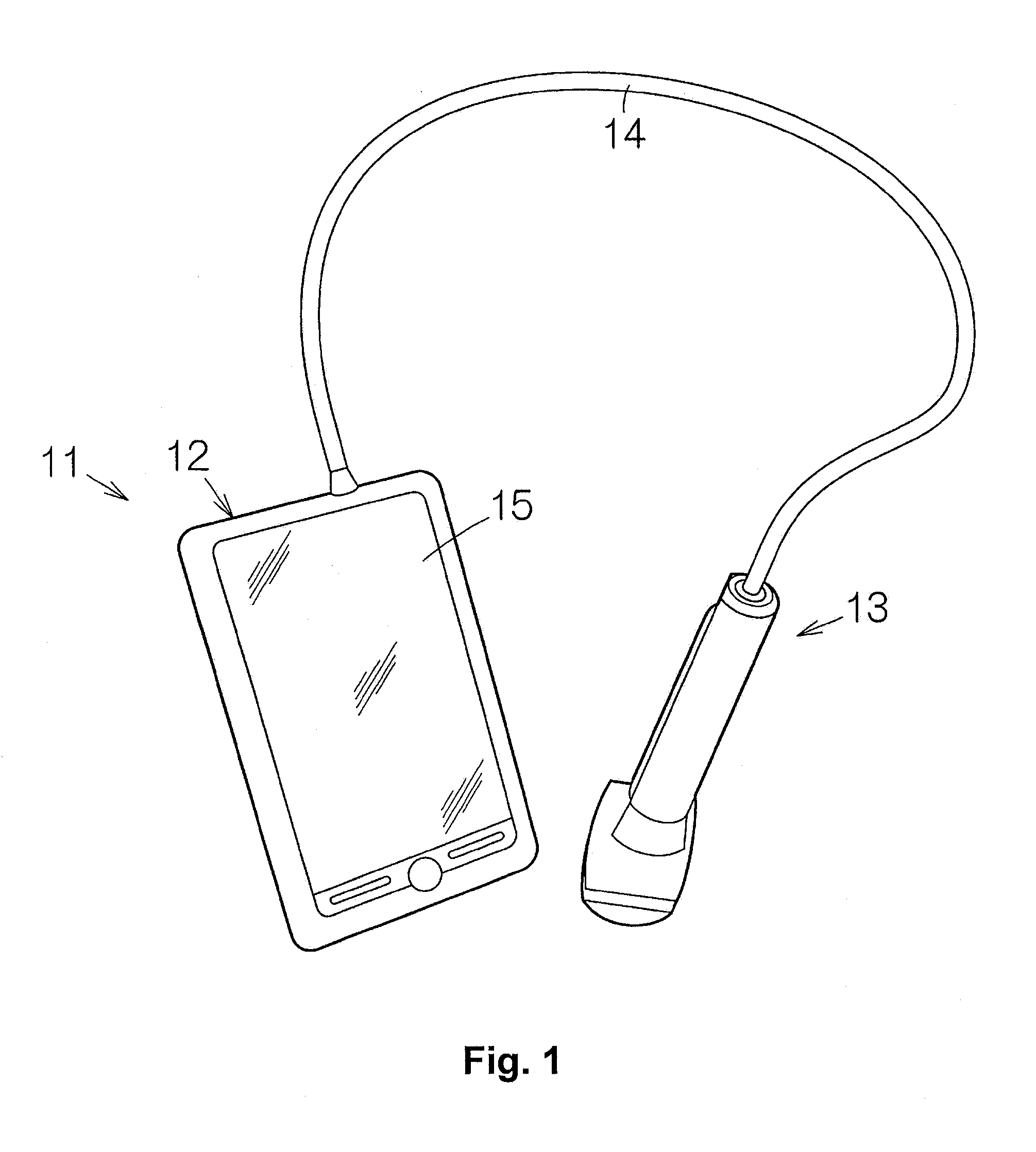
Ultrasonic transducer device, probe, electronic instrument, and ultrasonic diagnostic device
a transducer and ultrasonic technology, applied in ultrasonic/sonic/infrasonic image/data processing, ultrasonic/sonic/infrasonic diagnostics, mechanical vibration separation, etc., can solve the problems of further deterioration of strength of substrate, etc., to prevent complex manufacturing processes, reduce the distance between the ultrasonic transducer element and the pulser, and increase the rigidity of the wall
- Summary
- Abstract
- Description
- Claims
- Application Information
AI Technical Summary
Benefits of technology
Problems solved by technology
Method used
Image
Examples
second embodiment
(4) Configuration of Chip Unit
[0073]FIG. 7 schematically shows a configuration of the chip unit 17 according to a second embodiment of the present invention. The ultrasonic diagnostic device 11 can use an element chip 18a instead of the above-described element chip 18. In the second embodiment, the above-described integrated circuit is constructed of a monolithic integrated circuit 81 formed on the reverse surface of the wiring substrate 52 instead of the integrated circuit chip 55 of the first embodiment. Since the monolithic integrated circuit 81 is formed on the reverse surface of the wiring substrate 52, it can contribute to size reduction of the element chip 18a.
[0074]Although not illustrated in FIG. 7, the first wiring is formed on a reverse surface (second surface) of the wiring substrate 52 as in the first embodiment, and the monolithic integrated circuit 81, the external connection terminals 56, the relay terminals 58 are connected to the first wiring.
[0075]The other confi...
third embodiment
(5) Configuration of Chip Unit
[0076]FIG. 8 schematically shows a configuration of the chip unit 17 according to a third embodiment of the present invention. The ultrasonic diagnostic device 11 can use an element chip 18b instead of the above-described element chip 18. In the third embodiment, the integrated circuit chip 55 mounted on the first flexible printed circuit board 37 and (or) the second flexible printed circuit board 41. The integrated circuit chip 55 is connected to the conductive line of the first flexible printed circuit board 37 on the first flexible printed circuit board 37. The integrated circuit chip 55 is connected to the conductive line of the second flexible printed circuit board 41 on the second flexible printed circuit board 41. Since the integrated circuit chip 55 does not expand along a two-dimensional plane that includes the substrate 21, it can contribute to size reduction of the element chip 18b.
[0077]Although not illustrated in FIG. 8, the first wiring i...
fourth embodiment
(6) Configuration of Chip Unit
[0079]FIG. 9 schematically shows a configuration of the chip unit 17 according to a fourth embodiment of the present invention. The ultrasonic diagnostic device 11 can use an element chip 18c instead of the above-described element chip 18. In the fourth embodiment, a wiring substrate 82 is used instead of the above-described wiring substrate 52. The wiring substrate 82 receives the substrate 21 on the surface thereof. The reverse surface of the wiring substrate 82 is formed to be a flat surface. A first wiring 83 is formed on the surface of the wiring substrate 82. In order to form the first wiring 83, the wiring substrate 82 expands outwardly with respect to the outline of the substrate 21. The first wiring 83 can be made of a thin film of a conductive material. A metal material such as copper can be used as the conductive material. The thin film can draw a wiring pattern on the surface of the wiring substrate 82.
[0080]The first flexible printed circui...
PUM
 Abstract
Description
Claims
Application Information
 - R&D
- Intellectual Property
- Life Sciences
- Materials
- Tech Scout
- Unparalleled Data Quality
- Higher Quality Content
- 60% Fewer Hallucinations
Browse by: Latest US Patents, China's latest patents, Technical Efficacy Thesaurus, Application Domain, Technology Topic, Popular Technical Reports.
© 2025 PatSnap. All rights reserved.Legal|Privacy policy|Modern Slavery Act Transparency Statement|Sitemap|About US| Contact US: help@patsnap.com


