Organic Semiconducting Material and Electronic Component
a semiconducting material and organic technology, applied in the direction of non-metal conductors, conductors, synthetic resin layered products, etc., can solve the problems of undesired tolerances of products, undesired irregularities in electronic components, and high control and regulation efforts within, so as to improve thermal stability, reduce the effect of absorption and improved conductivity
- Summary
- Abstract
- Description
- Claims
- Application Information
AI Technical Summary
Benefits of technology
Problems solved by technology
Method used
Image
Examples
example 1
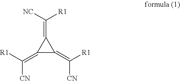
[0072]A layer of the HTM of formula 3 was doped with compound (p). The doped layer was deposited on a glass substrate coated with ITO by mixed evaporation of the HTM of formula 3 together with doping agent (p) under high vacuum. The concentration of the doping agent in the matrix was 1.5; 3.0; 4.5 wt %. In addition, an α-NPD layer doped with 3 wt % of compound (p) was deposited on the same substrate as a reference. Subsequently, a layer of α-NPD, a fluorescent blue emitter layer, an undoped ETL and blocking layer, an n-doped electron transport layer and an aluminum cathode were deposited without breaking the vacuum. The components processed in this way were then protected from water by encapsulating in a covering glass—an appropriate getter had been introduced in advance.
[0073]Blue OLEDs that emit through the glass substrate are thus produced, the characteristic data of said OLEDs being summarised in the table below.
CurrentPowerHTL:efficiencyefficiency / QuantumServiceServicedopingVol...
example 2
[0075]A layer of the HTM of formula 3 was doped with compound (p). The doped layer was deposited on a glass substrate coated with ITO by mixed evaporation of the HTM of formula 2 together with doping agent (p) under high vacuum. The concentration of the doping agent in the matrix was 3.0 wt %. In addition, an α-NPD layer doped with 3 wt % of compound (p) was deposited on the same substrate as a reference. Subsequently, a layer of α-NPD or a layer of the HTM of formula 3 was deposited without breaking the vacuum. The component was completed by a fluorescent red emitter layer, an undoped ETL and blocking layer, an n-doped electron transport layer and an aluminum cathode. The components processed in this way were then protected from water by encapsulating in a covering glass—an appropriate getter had been introduced in advance.
[0076]Red OLEDs that emit through the glass substrate are thus produced, the characteristic data of said OLEDs being summarised in the table below.
Power efficien...
example 3
[0078]A further component example shall demonstrate the surprising thermal stability of the doped semiconductor layers. To this end, a layer 30 nm thick layer of each of the HTM of formula 4, the HTM of formula 5 and the HTM of formula 6 was processed on ITO glass. In addition, a reference layer of 30 nm α-NPD was applied. All of these materials were doped electrically with (p) 3% by co-evaporation. A uniform layer 50 nm thick of a highly stable hole-transporting material TBRb (tert butyl rubrene) was evaporated as additional resistance on all of these layers. The hole-transporting components were terminated by a common aluminum electrode 100 nm thick. The components processed in this way were then protected from water by encapsulating in a covering glass—an appropriate getter had been introduced in advance.
[0079]The current-voltage characteristic curves of the components thus obtained were measured. For the purposes of estimating the thermal stability, all OLEDs were then heated in...
PUM
| Property | Measurement | Unit |
|---|---|---|
| Temperature | aaaaa | aaaaa |
| Temperature | aaaaa | aaaaa |
| Temperature | aaaaa | aaaaa |
Abstract
Description
Claims
Application Information
 - R&D
- Intellectual Property
- Life Sciences
- Materials
- Tech Scout
- Unparalleled Data Quality
- Higher Quality Content
- 60% Fewer Hallucinations
Browse by: Latest US Patents, China's latest patents, Technical Efficacy Thesaurus, Application Domain, Technology Topic, Popular Technical Reports.
© 2025 PatSnap. All rights reserved.Legal|Privacy policy|Modern Slavery Act Transparency Statement|Sitemap|About US| Contact US: help@patsnap.com


