Printed circuit board and method for manufacturing the same

a printed circuit board and manufacturing method technology, applied in the direction of printed circuit non-printed electric components association, final product manufacturing, resistive material coating, etc., can solve the problems of increasing the size of the module, implementing a fine pitch, and requiring additional processes, so as to improve the mounting stability of external elements

Inactive Publication Date: 2013-06-27
SAMSUNG ELECTRO MECHANICS CO LTD
View PDF2 Cites 15 Cited by
  • Summary
  • Abstract
  • Description
  • Claims
  • Application Information

AI Technical Summary

Benefits of technology

[0009]The present invention has been made in an effort to provide a printed circuit board (PCB) having enhanced mounting stability of external elements, and a method for manufacturing the same.
[0011]The present invention has also been made in an effort to provide a PCB in which a formation of voids is prevented during an underfill process, and a method for manufacturing the same.
[0018]According to another preferred embodiment of the present invention, there is provided a method for manufacturing a printed circuit board (PCB), including: preparing a base substrate on which a circuit layer including a connection pad is formed; forming a solder resist layer having a first opening exposing the connection pad on an upper portion of the base substrate; forming a first plated resist layer which has a second opening exposing the first opening and has a diameter greater than that of the first opening on an upper portion of the solder resist layer; forming a seed layer on an upper portion of the first plated resist layer, on an inner wall of the first opening, and on an inner wall of the second opening; forming a second plated resist layer which has a third opening exposing the first opening on an upper portion of the seed layer; plating the interior of the first through third openings to form a metal post; eliminating the second plated resist layer; eliminating the seed layer exposed through the elimination of the second plated resist layer; and eliminating the first plated resist layer exposed through the elimination of the seed layer.

Problems solved by technology

However, in the case of the wire bonding scheme, since the semiconductor chip is connected to the PCB by using a wire, the size of a module is increased, an additional process is required, and there is a limitation in implementing a fine pitch, so the flip chip bonding scheme is commonly used, instead.
However, as PCBs are becoming fine, an opening of a pad on which bumps are formed is reduced, causing problems such as a degradation of bonding strength between PCBs and bumps, a reduction in mounting stability, defective underfill, and the like.

Method used


Image

  • Printed circuit board and method for manufacturing the same
  • Printed circuit board and method for manufacturing the same
  • Printed circuit board and method for manufacturing the same

Examples


Embodiment Construction

[0029]Various features and advantages of the present invention will be more obvious from the following description with reference to the accompanying drawings.

[0030]The terms and words used in the present specification and claims should not be interpreted as being limited to typical meanings or dictionary definitions, but should be interpreted as having meanings and concepts relevant to the technical scope of the present invention based on the rule according to which an inventor can appropriately define the concept of the term to describe most appropriately the best method he or she knows for carrying out the invention.

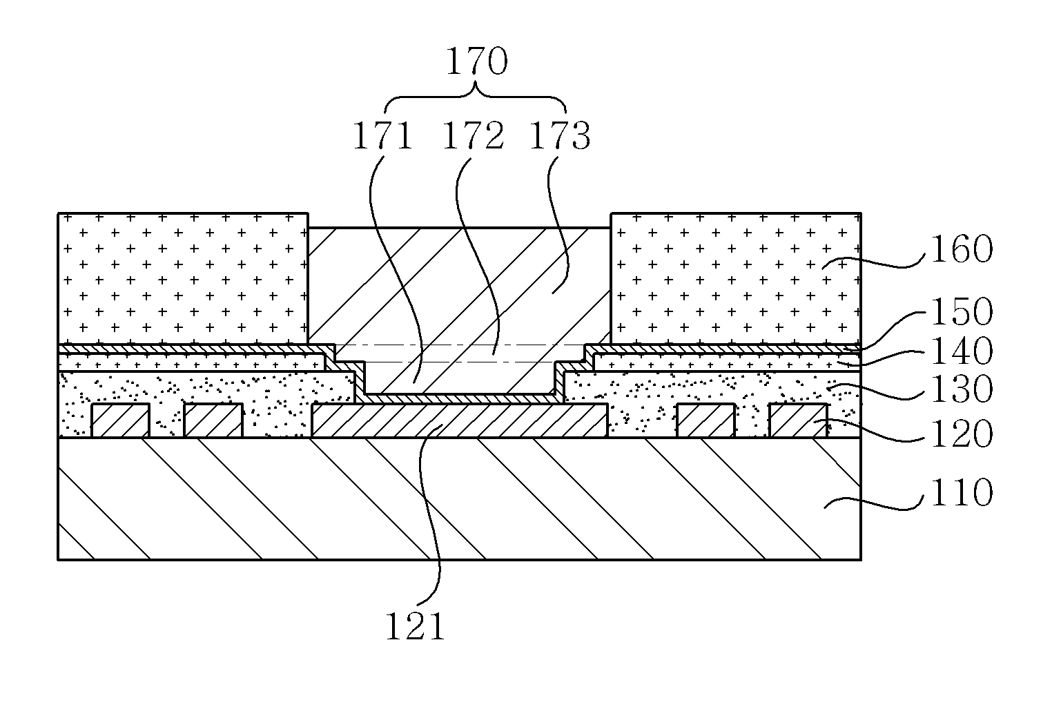
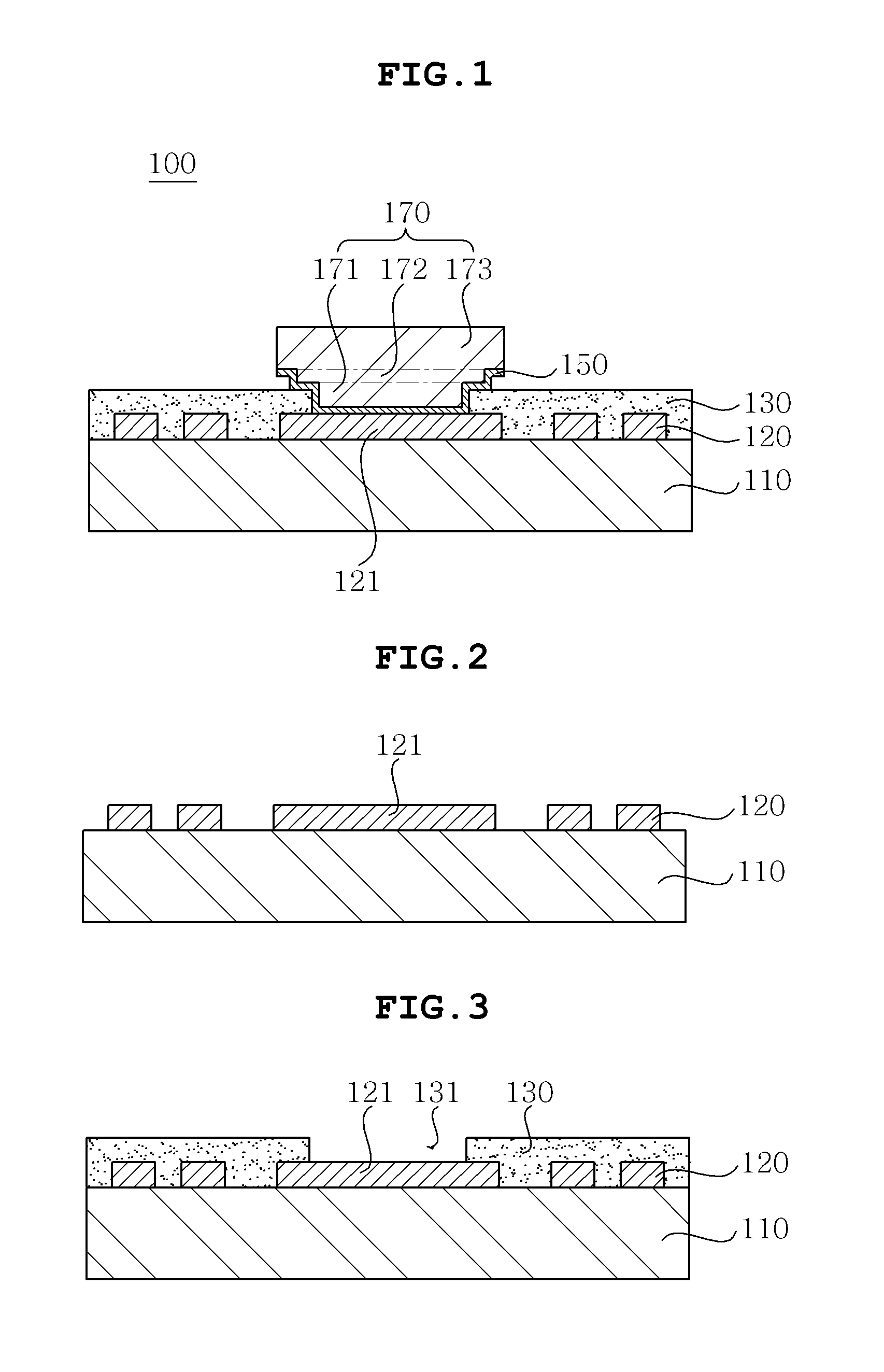
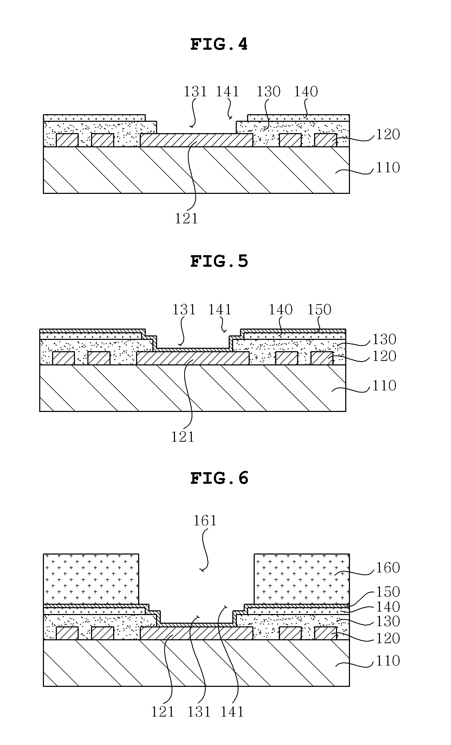
[0031]The above and other objects, features and advantages of the present invention will be more clearly understood from the following detailed description taken in conjunction with the accompanying drawings. In the specification, in adding reference numerals to components throughout the drawings, it is to be noted that like reference numerals designate like component...


PUM

PropertyMeasurementUnit
diametersaaaaaaaaaa
diameteraaaaaaaaaa
sizeaaaaaaaaaa

Abstract

Disclosed herein are a printed circuit board (PCB) and a method for manufacturing the same. The PCB includes a base substrate, a circuit layer formed on the base substrate and including a connection pad, a solder resist layer formed on an upper portion of the base substrate and having an opening exposing the connection pad, a metal post formed on upper portions of the connection pad and the solder resist layer and having a plurality of diameters, and a seed layer formed on the upper portion of the solder resist layer and inner walls of the opening along an interface of the metal post.

Description

CROSS REFERENCE TO RELATED APPLICATION[0001]This application claims the benefit of Korean Patent Application No. 10-2011-0140328, filed on Dec. 22, 2011, entitled “Printed Circuit Board and Manufacturing Method Thereof”, which is hereby incorporated by reference in its entirety into this application.BACKGROUND OF THE INVENTION[0002]1. Technical Field[0003]The present invention relates to a printed circuit board and a method for manufacturing the same.[0004]2. Description of the Related Art[0005]With the development of the electronics industry, electronic components are increasingly required to have high performance, be multifunctional and have a smaller size. According to the trend, requirements for substrates used for surface-mounted components such as a system in package (SIP), a 3D package, and the like, to become highly integrated and thinner and have a fine circuit pattern have emerged.[0006]In a surface mount technology for mounting external elements such as a semiconductor ch...

Claims


Application Information

Patent Timeline
Patent Type & Authority Applications(United States)
IPC IPC(8): H05K1/18H05K3/00
CPCH01L2224/831Y10T29/49165H01L21/563H01L24/11H01L24/13H01L24/81H01L2224/11462H01L2224/119H01L2224/11912H01L2224/13017H01L2224/13018H01L2224/13022H01L2224/131H01L2224/13139H01L2224/13144H01L2224/13147H01L2224/13155H01L2224/16227H01L2224/73204H01L2224/81192H01L2224/81801H01L2224/11474H01L2224/1184H01L2224/8138H05K2203/0588H05K2201/09845H05K3/4007H05K1/111H01L23/49894H01L23/49811H05K2203/054H05K2201/0367H01L2224/16225H01L2924/00014H01L2924/014Y02P70/50H01L2924/00012H05K3/34
Inventor OH, HUENG JAEJUNG, BOO YANGLEE, DAE YOUNGCHOI, JIN WON
Owner SAMSUNG ELECTRO MECHANICS CO LTD
Why Eureka
Try Eureka