
Room temperature glass-to-glass, glass-to-plastic and glass-to-ceramic/semiconductor bonding

a technology of glass-to-glass, glass-to-semiconductor and room temperature, which is applied in the direction of glue vessels, auxillary welding devices, welding/cutting auxillary devices, etc., can solve the problems of aggravated contamination problems, low bonding temperature, and process not very robust against environmental particles

Active Publication Date: 2013-05-09
CORNING INC
View PDF1 Cites 72 Cited by
  • Summary
  • Abstract
  • Description
  • Claims
  • Application Information

AI Technical Summary

Benefits of technology

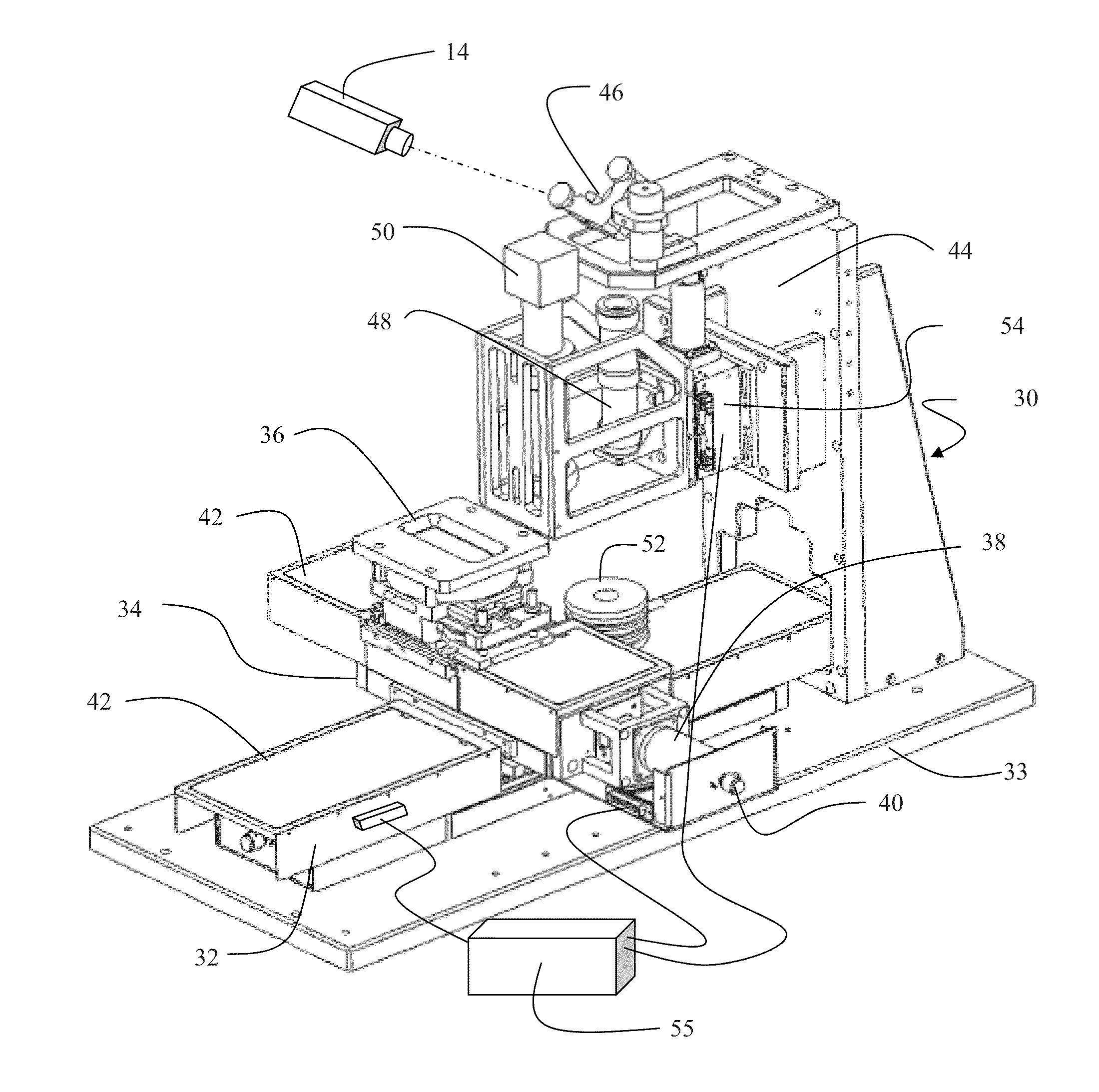
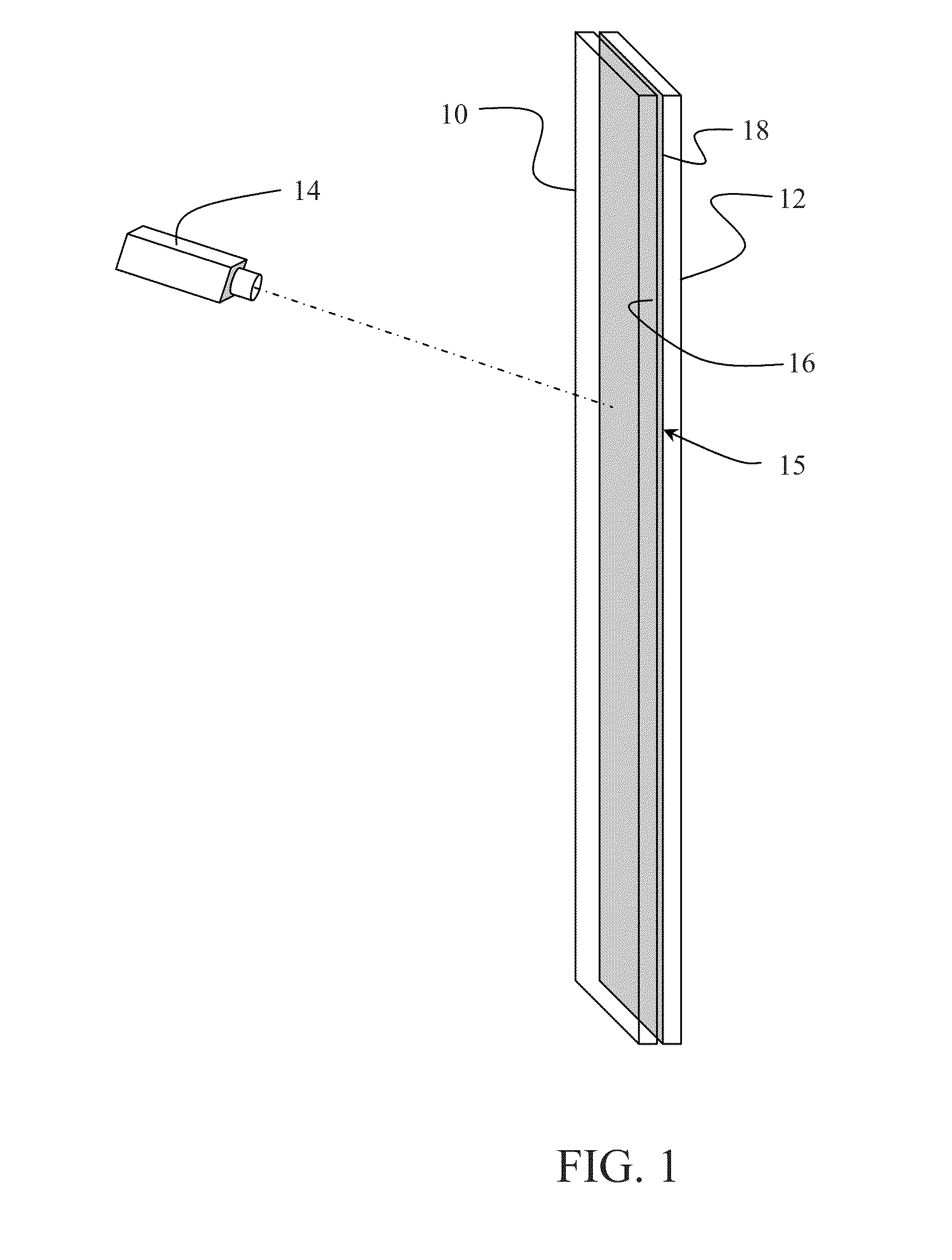
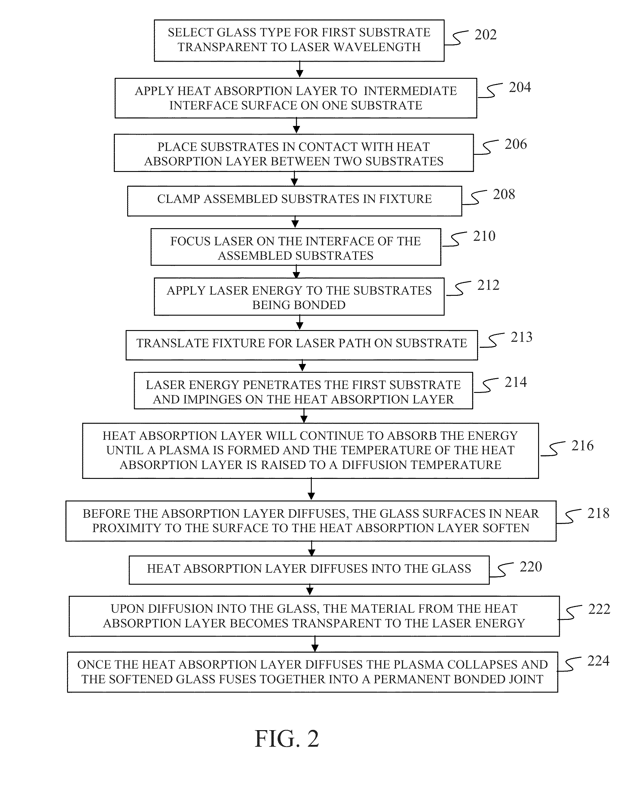
The patent text describes a process for bonding two substrates using a laser at room temperature. The process involves selecting two substrates, creating a change in index of transmission at the interface between the two substrates, and then mating the substrates together using a laser focused on the interface. The laser creates a high temperature at the interface, which softens the substrates and causes them to fuse. The process can be carried out using a blocking heat absorption coating or by differing the transmissivity of the substrates themselves. An apparatus for carrying out the process is also described, including an x-axis motion stage for aligning and securing the substrates, a gantry for supporting alignment optics, and a controller for translating the motion stages. Overall, the patent text provides a method and apparatus for room temperature substrate bonding using a laser that is efficient, flexible, and effective.

Problems solved by technology

This process is not very robust against environmental particles that are commonly found in a clean room environment.
Such treatments tend to lower the bonding temperatures but aggravate the contamination problem.
Contamination becomes more difficult because the particulate does not have the ability to deform the glass such that the particle of contamination will recess out of the way and not hold the two surfaces apart.
Fusion bonding has two competing issues that cause a low yield; the glass surface must be absolutely clean in order to not create air bubbles at low temperatures, and when higher temperatures are used, while air gaps become less a problem, the surface of the glass becomes distorted and must be reprocessed in order to make it optically clear again.
Higher temperatures can also cause the glass to become hazed or yellowish.
While there are a few exceptions, it is general y not possible to bond glass-to-glass with an Anodic bonding process.
Such a charge on the surface of the glass can easily interfere with downstream processes during the use of the chip.
While adhesive is easy to apply, it is very hard to make a bubble free joint.
It is also very hard to pattern adhesive such that the bond line is complete but does not squeeze out from between the surfaces being bonded and into a neighboring channel.
Adhesives can be hazardous to the downstream process.
Certain adhesive compositions can kill the biology that the component is being made to house.
In each case the bond lines are not robust against strong concentrations of acid or bases.
The higher etch rate can cause small crevasse that are hard to clean or harm the flow of liquid in the channel assembly in the case of micro-fluidics.
If this is not done, when the material returns to room temperature the bonded component will warp and / or break.
The adhesive joint will fail in shear or peel if the use temperature is different from the bonding temperature; adhesive shear strength is usually low.

Method used


Image

  • Room temperature glass-to-glass, glass-to-plastic and glass-to-ceramic/semiconductor bonding
  • Room temperature glass-to-glass, glass-to-plastic and glass-to-ceramic/semiconductor bonding
  • Room temperature glass-to-glass, glass-to-plastic and glass-to-ceramic/semiconductor bonding

Examples


example 1

Substrates of Different Thermal Coefficient of Expansion (TCE)

[0040]Traditional bonding processes typically occur at elevated temperatures, where a vastly different TCE generates severe temperature distortion when the bonded assembly cools down. However, with laser bonding process disclosed herein it is possible to bond dissimilar TCE materials at the temperature. Since the bulk temperature of the material being bonded can be set at the temperature of use, the TCE while still being different does not stress or otherwise distort the substrate material because it does not see a temperature change.

[0041]For example when fusion bonding two substrates that are 150 mm in diameter with a TCE that differs by 7 ppm / °C. at a temperature of 100° C. The differential change in length from the top to the bottom substrate causes an engineering strain of 0.07% translating into a tensile stress in the bottom substrate of 54.6 Mpa (7.92 kpsi). Most glasses, for example, will fail in tension between 1...

example 2

Different Light Transmission at a Similar Laser Radiation Wave Length

[0043]It is a common practice to bond glass packaging to a silicon chip. When performing this process, it is usually necessary to match the CTE of each of the materials and to use a glass material with sodium atoms that can migrate during the elevated temperature bonding process. While there are commercially available glass materials that exhibit such properties, they are hard to process during such steps as introducing a via. Photo-sensitive glass ceramic material, such as Forturan, is easy to structure; however, it has a CTE of 10 ppm / °C. and does not contain sodium ions. These two attributes make it nearly impossible to anodic bond to silicon. While it can be fusion bonded, it requires being heated to 500° C. Such a high temperature change will cause the glass-silicon assembly to fracture during the cool down process.

[0044]While diffusion or Anodic bonding Forturan to Silicon is not practical, the laser bond pro...

example 3

Glass-to-Plastic Bonding

[0046]Glass to plastic bonding is very similar to the above process with one limitation; the blocking layer should be a relatively low temperature diffusion material such that it does not melt the polymer being attached to the glass. A particularly good material with a low diffusion temperature is AuSn (gold-tin eutectic). A gold-tin blocking heat absorption layer has a diffusion temperature of 280° C. Another helpful attribute is that the laser-pulse-width approaches the thermal-time-constant of the blocking heat absorption layer layer, i.e., in the femto-second regime. The shorter the pulse length, the less likelihood there is to burn or melt the polymer prior to bonding the high-melting-temperature glass material to the lower temperature melting plastic material. It is also possible to use infared laser radiation without an interlayer and use the blocking nature of the polymer at this wavelength to perform the bonding.


PUM

PropertyMeasurementUnit
Fractionaaaaaaaaaa
Temperatureaaaaaaaaaa
Electrical conductoraaaaaaaaaa

Abstract

A process for room temperature substrate bonding employs a first substrate substantially transparent to a laser wavelength is selected. A second substrate for mating at an interface with the first substrate is then selected. A transmissivity change at the interface is created and the first and second substrates are mated at the interface. The first substrate is then irradiated with a laser of the transparency wavelength substantially focused at the interface and a localized high temperature at the interface from energy supplied by the laser is created. The first and second substrates immediately adjacent the interface are softened with diffusion across the interface to fuse the substrates.

Description

BACKGROUND INFORMATION[0001]1. Field[0002]Embodiments of the disclosure relate generally to the field of bonding of transparent substrates and more particularly to a method for room temperature laser bonding of a first laser wavelength transparent substrate to a second substrate with an intermediate heat absorption layer.[0003]2. Background[0004]Bonding of glass-to-glass substrates and other combinations of transparent and non-transparent substrates for biological slides and microfluidics applications as well as other applications typically requires heating of the substrates to obtain bonding diffusion of the materials across the substrate boundaries unless adhesives are employed. Various examples of current bonding practices are fusion bonding, anodic bonding of sodium rich glass to semiconductors and adhesive bonding.[0005]Fusion bonding glass-to-glass is effective on polished, or low roughness glass surfaces. To achieve a strong, bubble free bond, typically the surface finish sho...

Claims


Application Information

Patent Timeline
IPC IPC(8): C23F1/00B32B37/06
CPCB32B37/06C03C27/00B32B2310/0843B32B2315/08C03B23/203B29C65/1612B29C65/1635B29C65/1638B29C65/1654B29C65/1683B29C65/7841B29C65/7847B29C66/1122B29C66/45B29C66/7465B23K26/032B23K26/046B23K26/063B23K26/0807B23K26/0853B23K26/203B23K26/246B23K26/3266B23K2201/18B23K2201/40B23K2203/18B01L3/502707B01L2300/0887B32B2307/412B23K26/0622B23K26/082B23K26/211B23K26/244B23K2103/50B23K26/32B23K2103/18B23K2101/18B23K2101/40B29C66/7392B29C66/73161B23K2103/52B23K2103/42B23K2103/54B23K1/0056B23K1/19B23K26/324B23K37/0443B23K37/0435Y10T428/31601B01L2200/12
Inventor KARAM, RAYMOND MILLERROUSSOS, GEORGESFINKLE, MARKHARVEY, DANIELLA M.ACKERMANN-KARAM, PASCAL R.
Owner CORNING INC
Learn More