Method and apparatus for fabricating silicon heterojunction solar cells
- Summary
- Abstract
- Description
- Claims
- Application Information
AI Technical Summary
Benefits of technology
Problems solved by technology
Method used
Image

Examples
Embodiment Construction
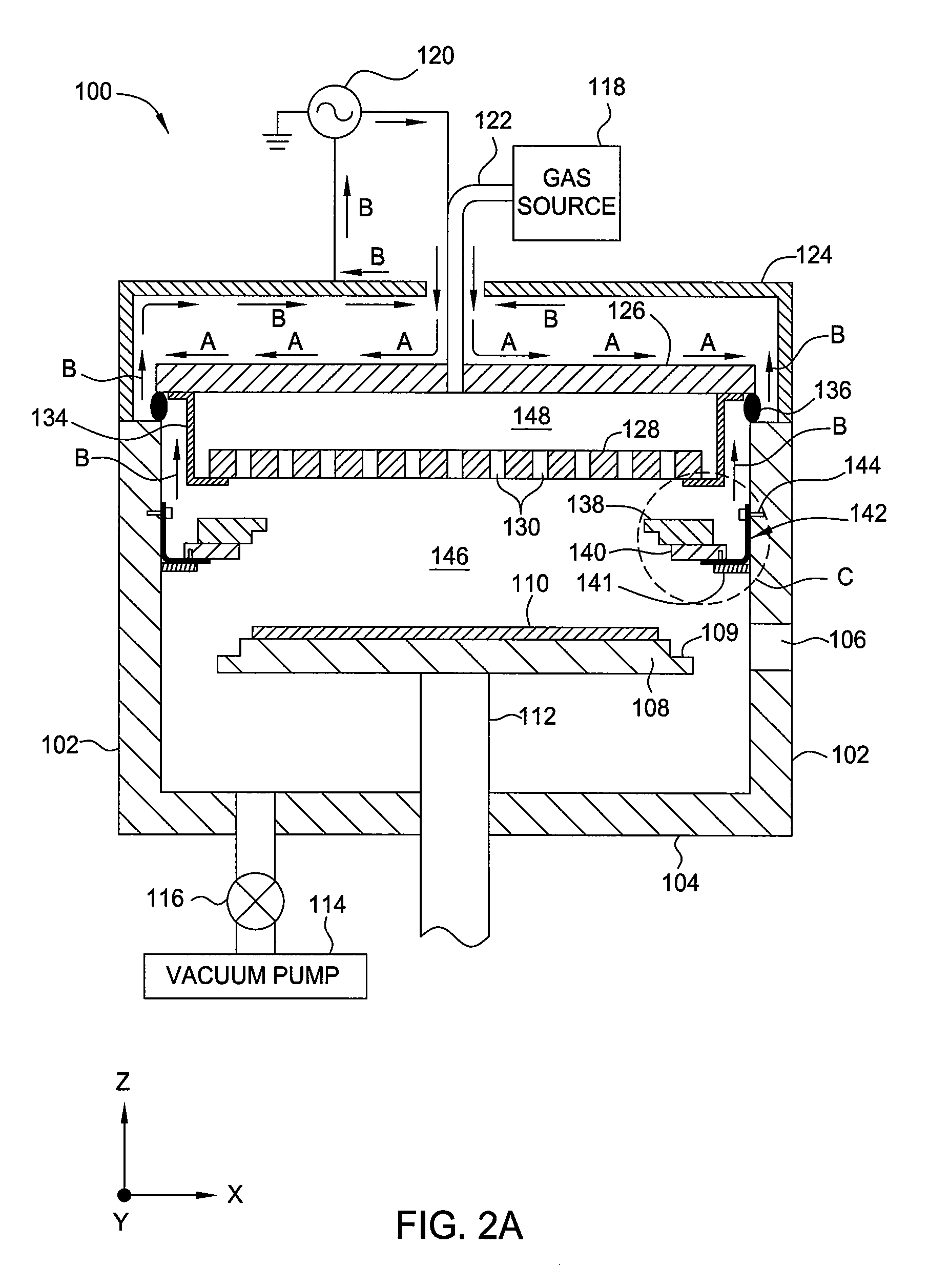
[0031]Embodiments of the present invention generally provide a processing system for deposition of semiconductor thin-films having low process-induced damage and a high degree of uniformity. In particular, it has been discovered that, in contrast to conventional radio frequency (RF) plasma enhanced chemical vapor deposition (PECVD) processes which utilize RF frequencies of less than about 30 MHz, semiconductor layers deposited via very high frequency (VHF) PECVD (approximately 30 to 300 MHz) display a low degree of plasma, charge, and thermal damage, resulting in films which exhibit superior interface passivation quality, increased doping efficiency, and an increase in overall heterojunction cell efficiency. Moreover, reduced deposition rates have improved thickness control and process repeatability. Finally, the unique process sequences used to fabricate the thin-film heterojunction layers allow for lower production costs and increased throughput (>2700 wafers / hour).
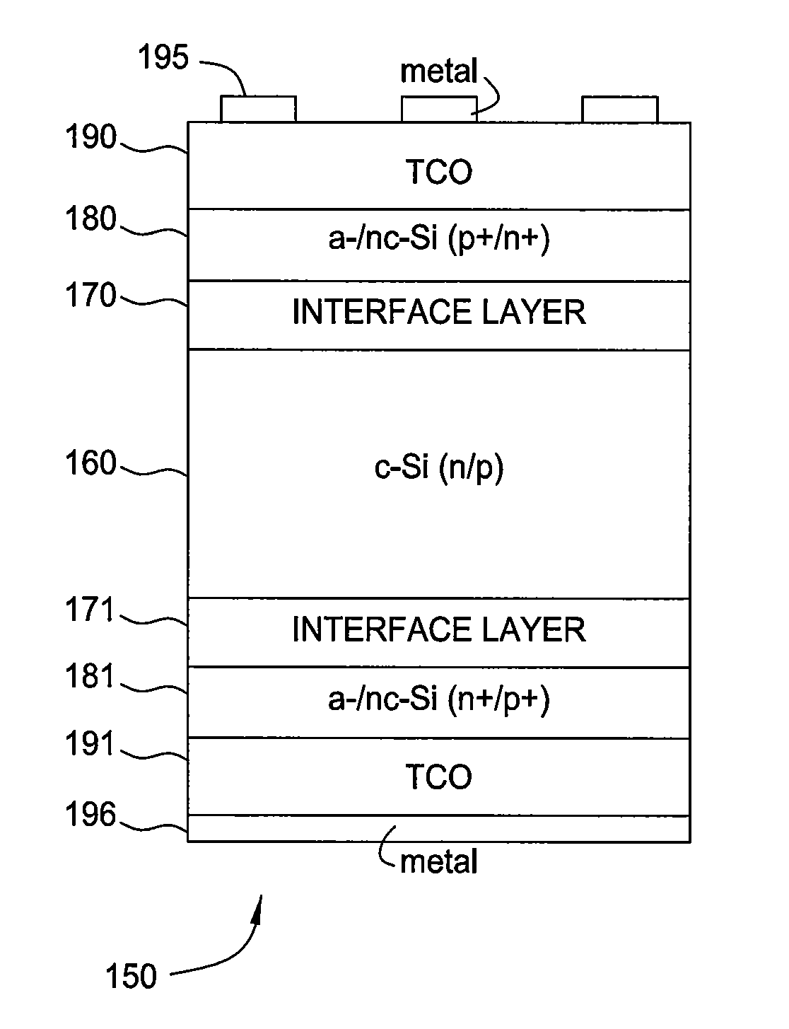
[0032]FIG. 1 is...
PUM
| Property | Measurement | Unit |
|---|---|---|
| Frequency | aaaaa | aaaaa |
| Frequency | aaaaa | aaaaa |
| Frequency | aaaaa | aaaaa |
Abstract
Description
Claims
Application Information
 - R&D
- Intellectual Property
- Life Sciences
- Materials
- Tech Scout
- Unparalleled Data Quality
- Higher Quality Content
- 60% Fewer Hallucinations
Browse by: Latest US Patents, China's latest patents, Technical Efficacy Thesaurus, Application Domain, Technology Topic, Popular Technical Reports.
© 2025 PatSnap. All rights reserved.Legal|Privacy policy|Modern Slavery Act Transparency Statement|Sitemap|About US| Contact US: help@patsnap.com