High-endurance phase change memory devices and methods for operating the same
- Summary
- Abstract
- Description
- Claims
- Application Information
AI Technical Summary
Benefits of technology
Problems solved by technology
Method used
Image
Examples
Embodiment Construction
[0021]A detailed description of embodiments of the present invention is provided with reference to the FIGS. 1-6.
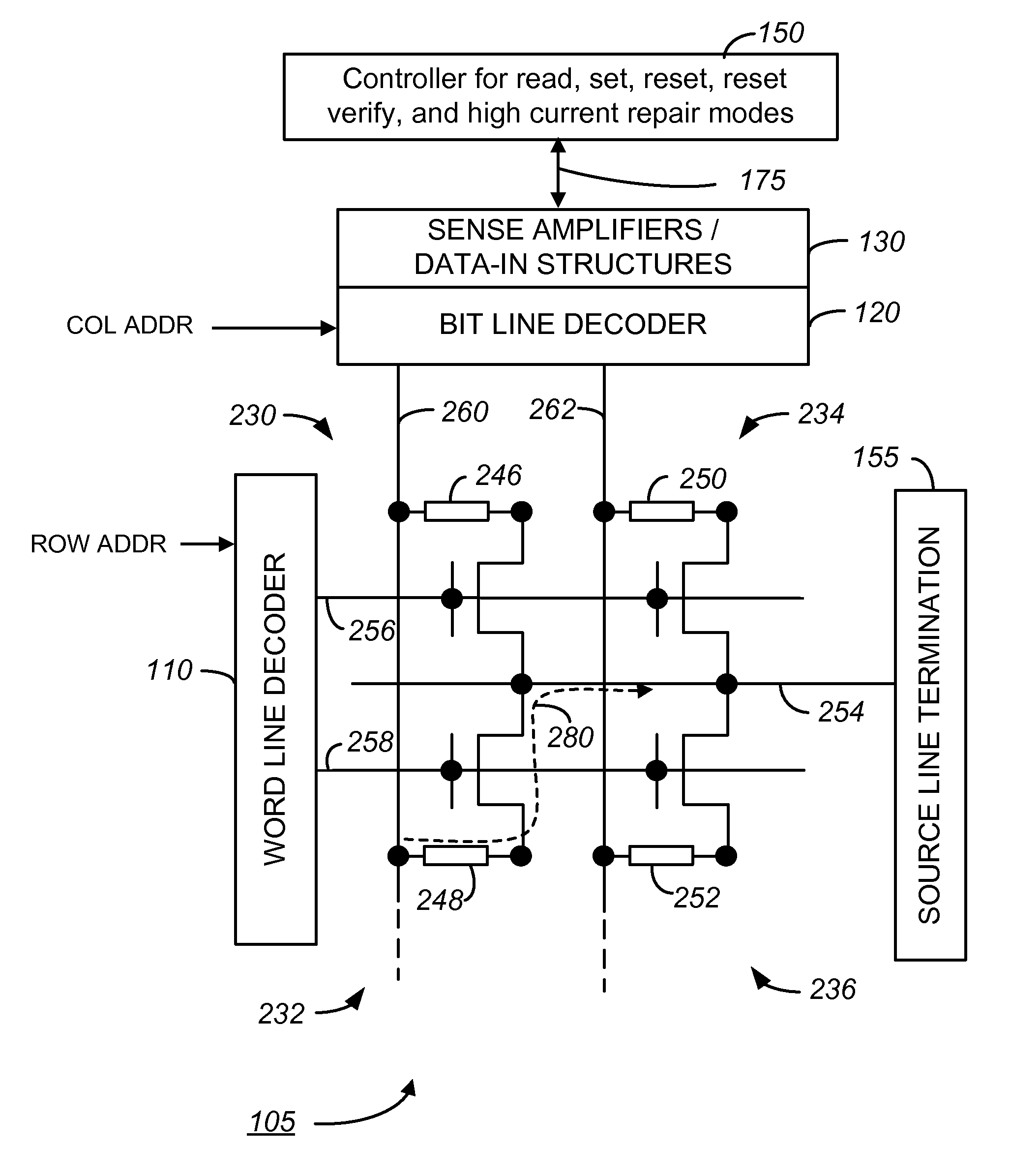
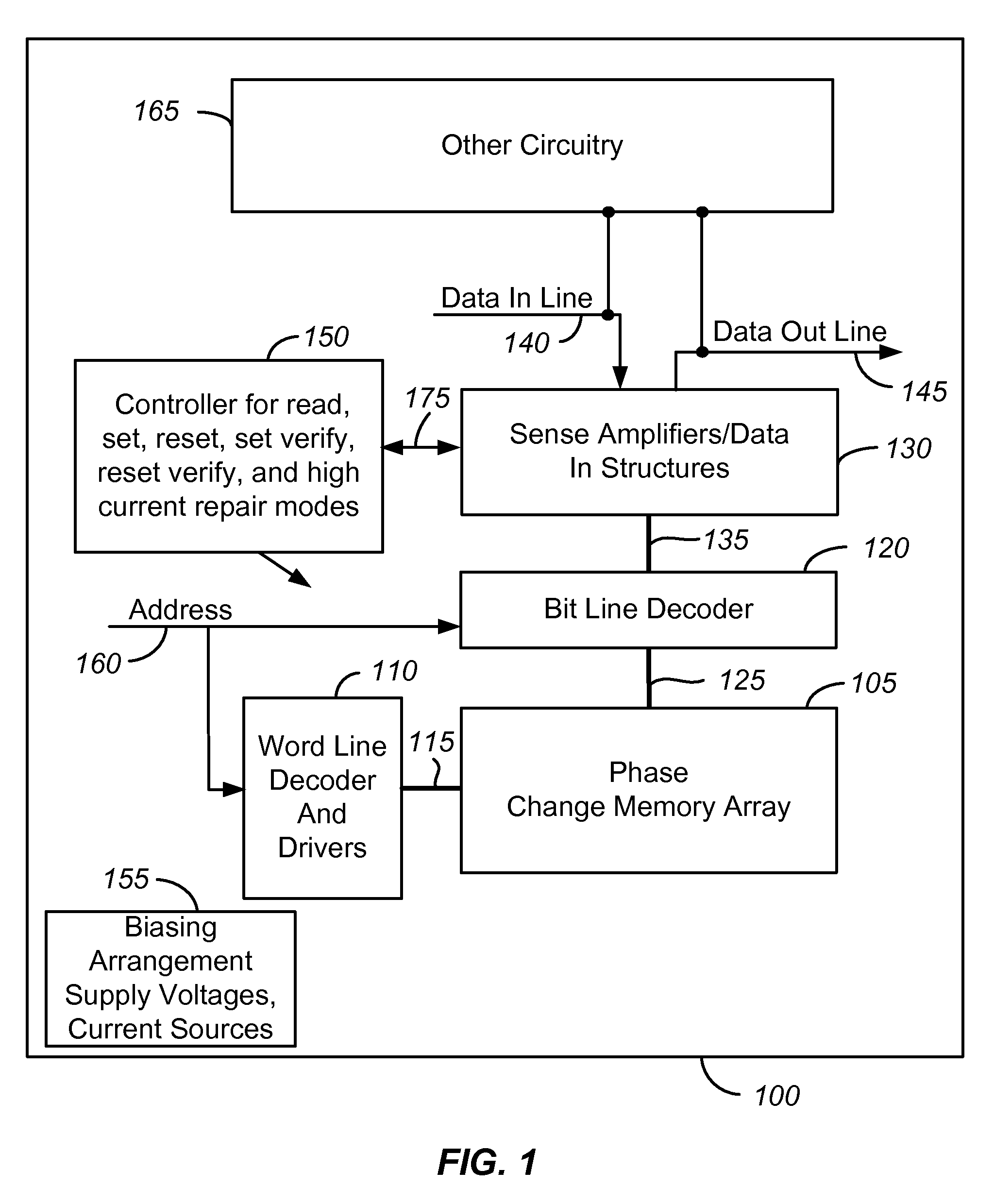
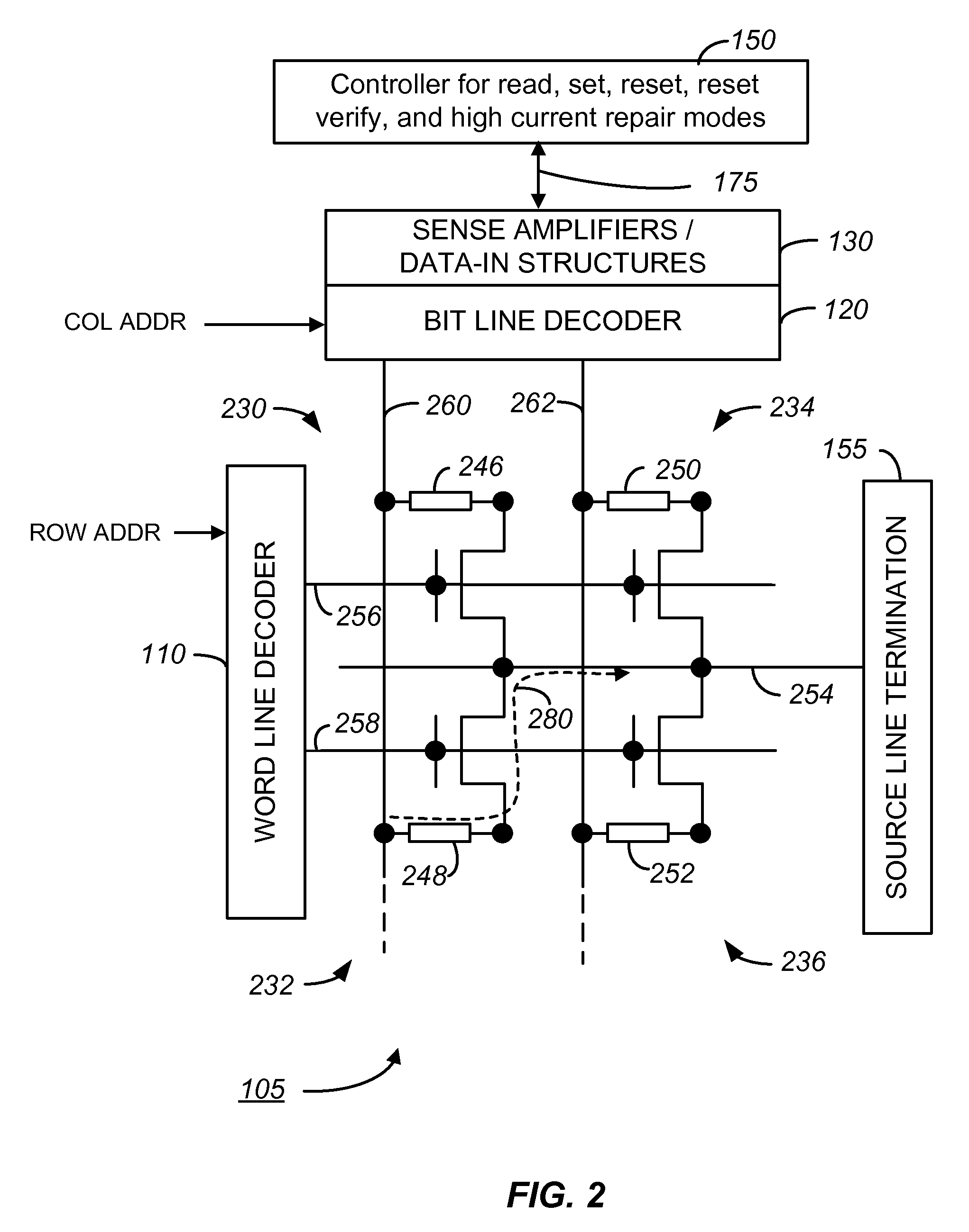
[0022]FIG. 1 is a simplified block diagram of an integrated circuit 100 including a phase change memory array 105 of phase change memory cells (not shown) which can be operated as described herein. A word line decoder and drivers 110 having read, set, reset, set verify, reset verify and high current repair modes is coupled to and in electrical communication with a plurality of word lines 115 arranged along rows in the phase change memory array 105. A bit line (column) decoder 120 is in electrical communication with a plurality of bit lines 125 arranged along columns in the array 105 for reading data from, and writing data to, the phase change memory cells in the array 105. Addresses are supplied on bus 160 to word line decoder and drivers 110 and bit line decoder 120. Sense circuitry (sense amplifiers) and data-in structures in block 130 are coupled to bit line decoder 12...
PUM
 Abstract
Description
Claims
Application Information
 - R&D
- Intellectual Property
- Life Sciences
- Materials
- Tech Scout
- Unparalleled Data Quality
- Higher Quality Content
- 60% Fewer Hallucinations
Browse by: Latest US Patents, China's latest patents, Technical Efficacy Thesaurus, Application Domain, Technology Topic, Popular Technical Reports.
© 2025 PatSnap. All rights reserved.Legal|Privacy policy|Modern Slavery Act Transparency Statement|Sitemap|About US| Contact US: help@patsnap.com


