Semiconductor process

Inactive Publication Date: 2012-12-06
NAN YA TECH
View PDF7 Cites 1 Cited by
  • Summary
  • Abstract
  • Description
  • Claims
  • Application Information

AI Technical Summary

Benefits of technology

[0005]The invention is directed to a semiconductor process, which forms the contact holes with desired profiles and reduces the fabrication cost and the processing time of the semiconductor device.
[0018]Based on the above, in the semiconductor process of the invention, the contact holes disposed in the memory region are formed by using a photomask, and the contact holes exposing the gates in the periphery region and the contact holes exposing the doped regions in the periphery region are formed simultaneously by using another photomask. As such, the contact holes have desired profiles respectively and the fabrication cost and the processing time of the semiconductor device is reduced.

Problems solved by technology

However, when an etching process is applied to form these contact holes simultaneously, over-etching or under-etching of the layers may be occurred because the material and the thickness of the layers required to be removed are not identical.
As such, electrical connection between the contact plugs formed in the contact holes and the devices is negatively affected, and the characteristics of the semiconductor device are deteriorated.
Otherwise, if the contact holes are defined respectively by different photomasks, the fabrication cost and the processing time are increased.

Method used


Image

  • Semiconductor process
  • Semiconductor process
  • Semiconductor process

Examples


Embodiment Construction

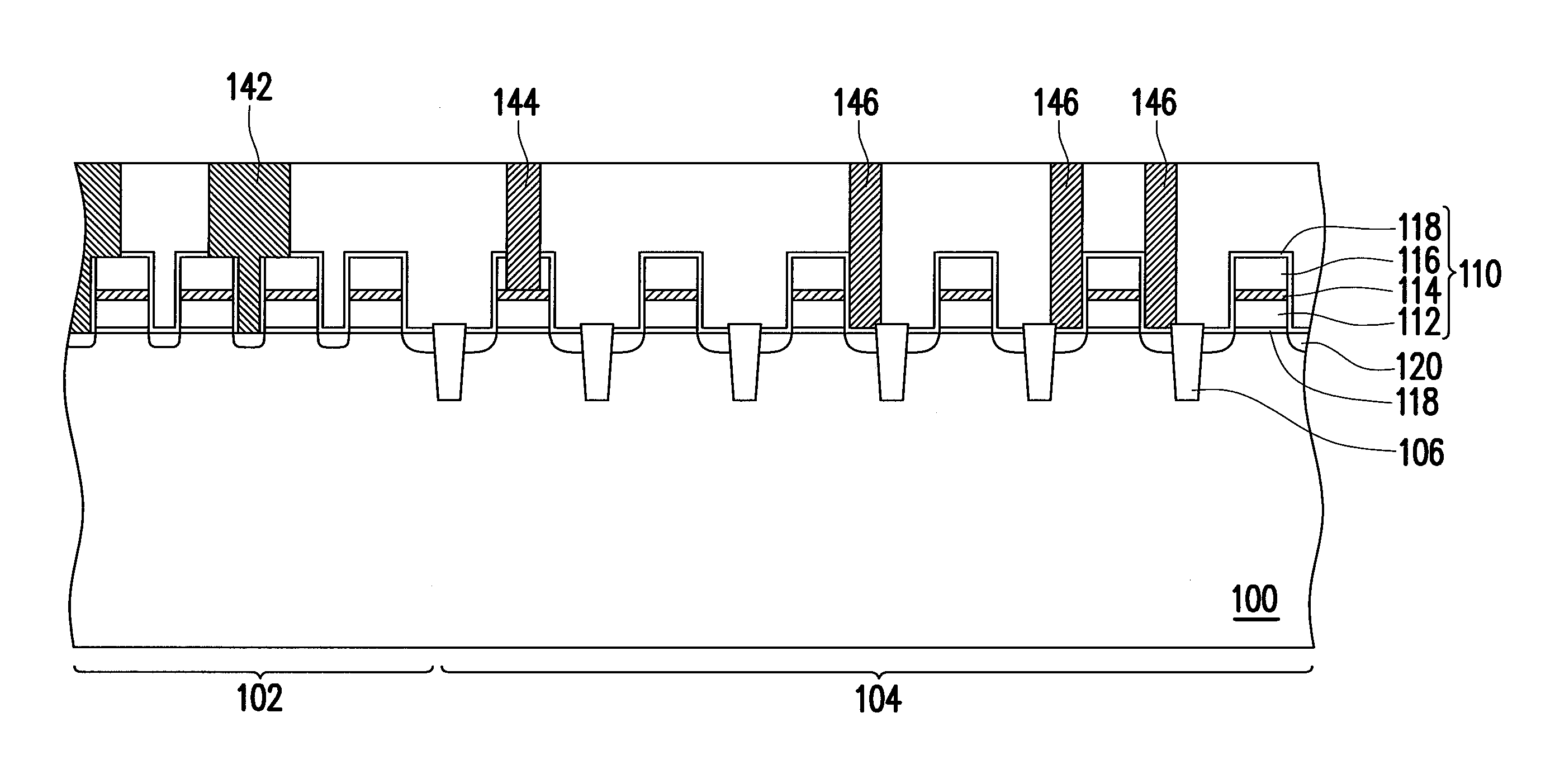
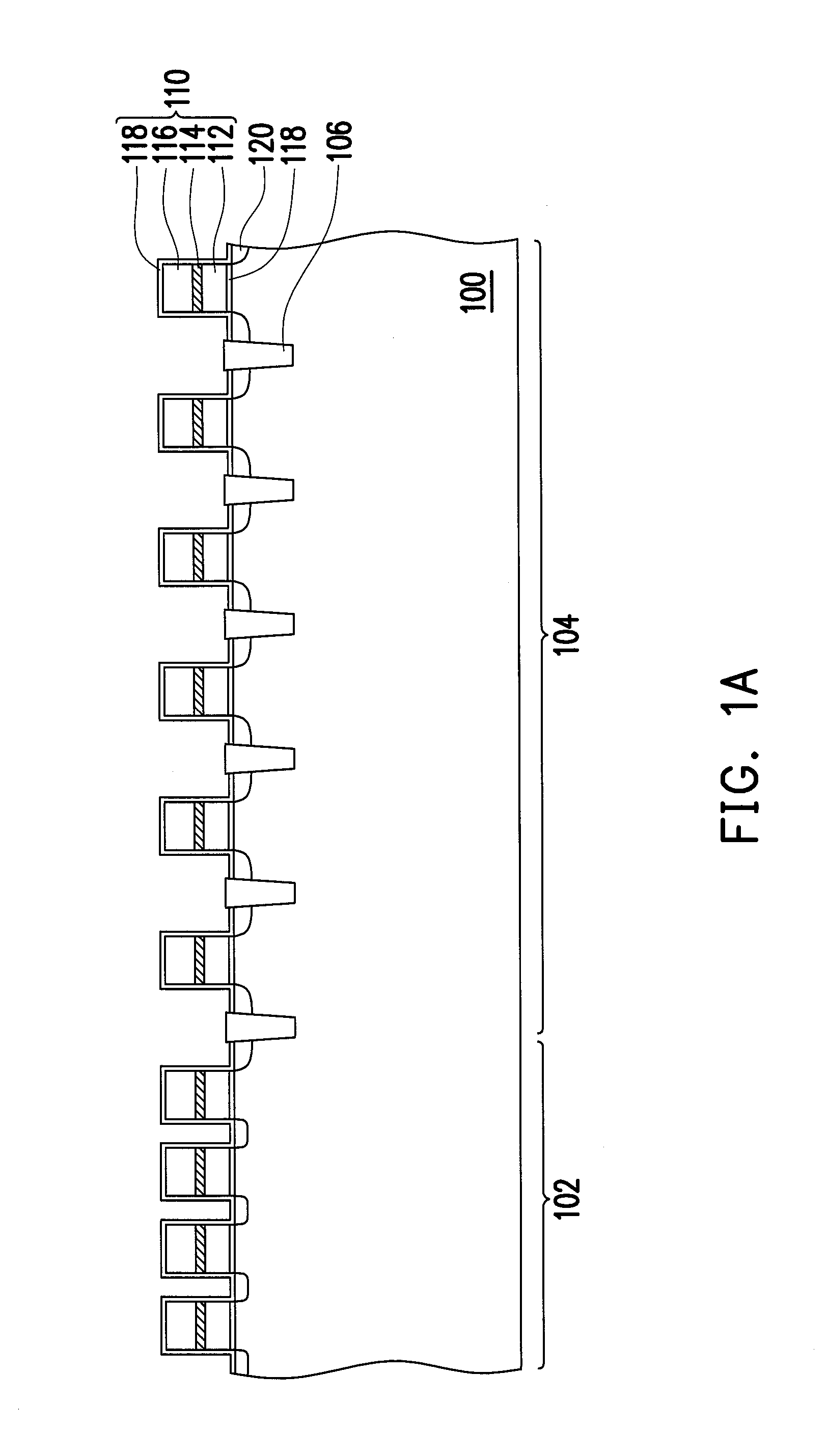
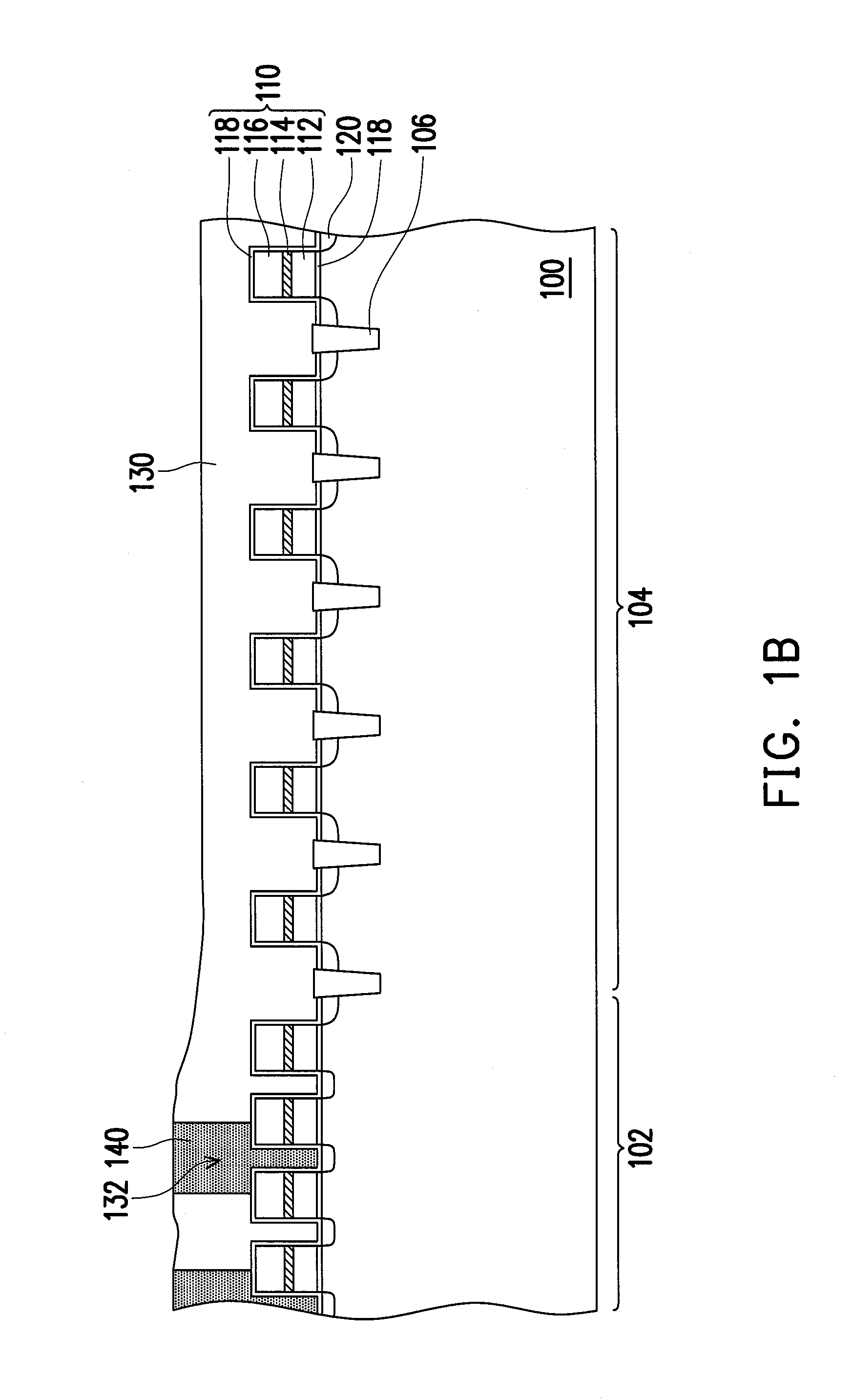
[0022]FIG. 1A to FIG. 1F are cross-sectional views illustrating a semiconductor process according to an embodiment of the invention. With reference to FIG. 1A, a substrate 100 is provided, wherein the substrate 100 includes a memory region 102 and a periphery region 104, a plurality of gates 110 is formed on the substrate 100, doped regions 120 are formed at two sides of each gate 110, and each gate 110 includes a silicon layer 112, a silicide layer 114 and a cap layer 116 sequentially formed on the substrate 100. In this embodiment, the substrate 100 is, for example, a silicon substrate, and a plurality of STI structure is formed therein. The doped regions 120 are source and drain regions, for example. In this embodiment, a material of the silicide layers 114 is, for example, WSi2, TiSi2, CoSi2, NiSi2 or any other suitable silicide material. A material of the cap layers 116 is, for example, nitride. In this embodiment, a gate dielectric layer 118 is disposed on a surface of each ga...


PUM


Abstract

A semiconductor process is provided. A substrate is provided, gates each including a silicon layer, a silicide layer and a cap layer are formed thereon, and doped regions are formed at two sides of each gate. An insulating layer is formed to cover a memory region and a periphery region. First contact holes are formed in the insulating layer in the memory region, and each first contact hole is disposed between the two adjacent gates and exposes the doped region. A contact plug is formed in each first contact hole to electrically connect the doped region. A patterned mask layer is formed on the substrate to cover the memory region and expose a portion of the periphery region. Using the patterned mask layer as a mask, second and third contact holes are formed in the insulating layer in the periphery region, to expose the silicide layer and the doped region.

Description

BACKGROUND OF THE INVENTION[0001]1. Field of the Invention[0002]The invention relates to a semiconductor process.[0003]2. Description of Related Art[0004]In the semiconductor process, in order to reduce number of photomasks, one photomask is used to simultaneously defined a plurality of contact holes in the insulating layer, including the contact holes disposed between the bit lines, the contact holes exposing the gates in the periphery region, and the contact holes exposing the source and drain regions in the periphery region. However, when an etching process is applied to form these contact holes simultaneously, over-etching or under-etching of the layers may be occurred because the material and the thickness of the layers required to be removed are not identical. As such, electrical connection between the contact plugs formed in the contact holes and the devices is negatively affected, and the characteristics of the semiconductor device are deteriorated. Otherwise, if the contact...

Claims


Application Information

Patent Timeline
IPC IPC(8): H01L21/8239
CPCH01L27/1052H01L21/76816H01L21/76897H10B99/00
Inventor WANG, WEN-CHIEHCHEN, YI-NANLIU, HSIEN-WEN
Owner NAN YA TECH
Why Eureka
Try Eureka