Organic light emitting device
a light-emitting device and organic technology, applied in the direction of organic semiconductor devices, solid-state devices, thermoelectric devices, etc., can solve the problems of unbalanced electrons and the number of injected holes, breakdown or instability of the electrode interface, and inability to achieve the effective combination of electrons and holes, etc., to achieve better luminous efficiency and stability
- Summary
- Abstract
- Description
- Claims
- Application Information
AI Technical Summary
Benefits of technology
Problems solved by technology
Method used
Image


Examples
first embodiment
The First Embodiment
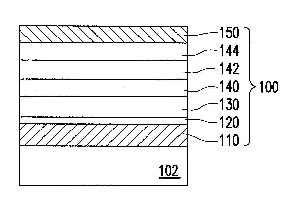
[0015]FIG. 1 is schematic cross-sectional view illustrating an organic light emitting device according to the first embodiment of the invention. Referring to FIG. 1, an organic light emitting device 100 is suitable for being disposed on a substrate 102. The organic light emitting device 100 includes a cathode layer 110, a buffer layer 120, a material layer 130, an organic light emitting layer 140 and an anode layer 150. The organic light emitting device 100 is, for example, an inverted organic light emitting device. According to the present embodiment, the organic light emitting device 100 is suitable for connecting with the drain of the n-type transistor in the driver circuit system of the display, for example.
[0016]The cathode layer 110 is disposed on the substrate 102. The substrate 102 can be made of glass, quartz, an organic polymer, plastic, flexible plastic, light-shielding materials, or reflective materials, and is not limited by the present invention. Th...
second embodiment
The Second Embodiment
[0023]FIG. 2 is schematic cross-sectional view illustrating an organic light emitting device according to the second embodiment of the invention. Referring to FIG. 2, an organic light emitting device 100 is suitable for being disposed on a substrate 102. The organic light emitting device 100 includes a cathode layer 110, a buffer layer 120, a material layer 130, an electron transporting layer 132, an organic light emitting layer 140 and an anode layer 150.
[0024]The cathode layer 110 is disposed on the substrate 102. The buffer layer 120 is disposed on the cathode layer 110 and contacts the cathode layer 110. According to the present embodiment, the cathode layer 110 is disposed between the substrate 102 and the buffer layer 120, that is, the organic light emitting device 100 is an inverted organic light emitting device. The material layer 130 is disposed on the buffer layer 120 and contacts the buffer layer 120. The difference between the lowest unoccupied molec...
experimental example
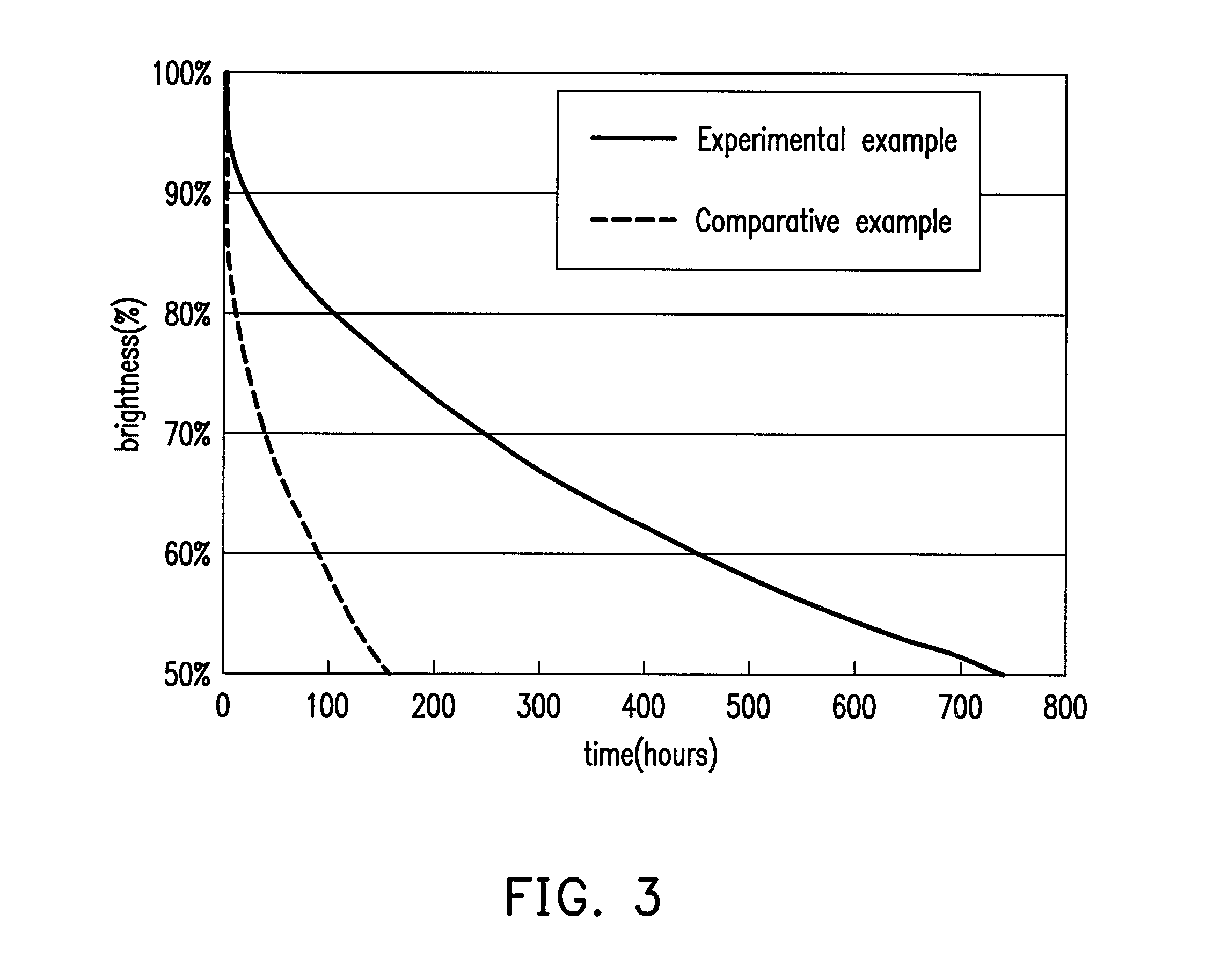
[0030]In order to verify that the organic light emitting device according to the above embodiments has better device characteristics, an experimental example is compared with a comparative example. The organic light emitting device according to the experimental example has a structure as shown in FIG. 1, wherein the cathode layer includes indium tin oxide and has a work function value of 5.0 eV, the buffer layer includes F4-TCNQ and has a LUMO of −5.3 eV and a thickness of 10 nm, the electron transporting layer includes Li-doped tris(8-quinolinato-N1,08)-aluminum (Alq:Li), the organic light emitting layer includes mCP:Ir(ppy)3, the hole transporting layer includes TCTA, the hole injecting layer includes m-MTDATA:F4-TCNQ, and the anode layer includes aluminum. The organic light emitting device according to the comparative example has a structure similar to that of the organic light emitting device according to the experimental example, and the difference lies in the organic light emi...
PUM
 Abstract
Description
Claims
Application Information
 - R&D
- Intellectual Property
- Life Sciences
- Materials
- Tech Scout
- Unparalleled Data Quality
- Higher Quality Content
- 60% Fewer Hallucinations
Browse by: Latest US Patents, China's latest patents, Technical Efficacy Thesaurus, Application Domain, Technology Topic, Popular Technical Reports.
© 2025 PatSnap. All rights reserved.Legal|Privacy policy|Modern Slavery Act Transparency Statement|Sitemap|About US| Contact US: help@patsnap.com