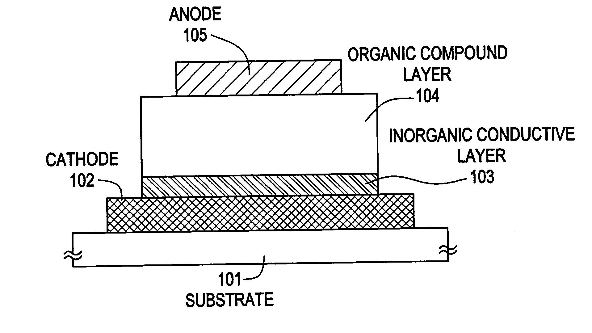
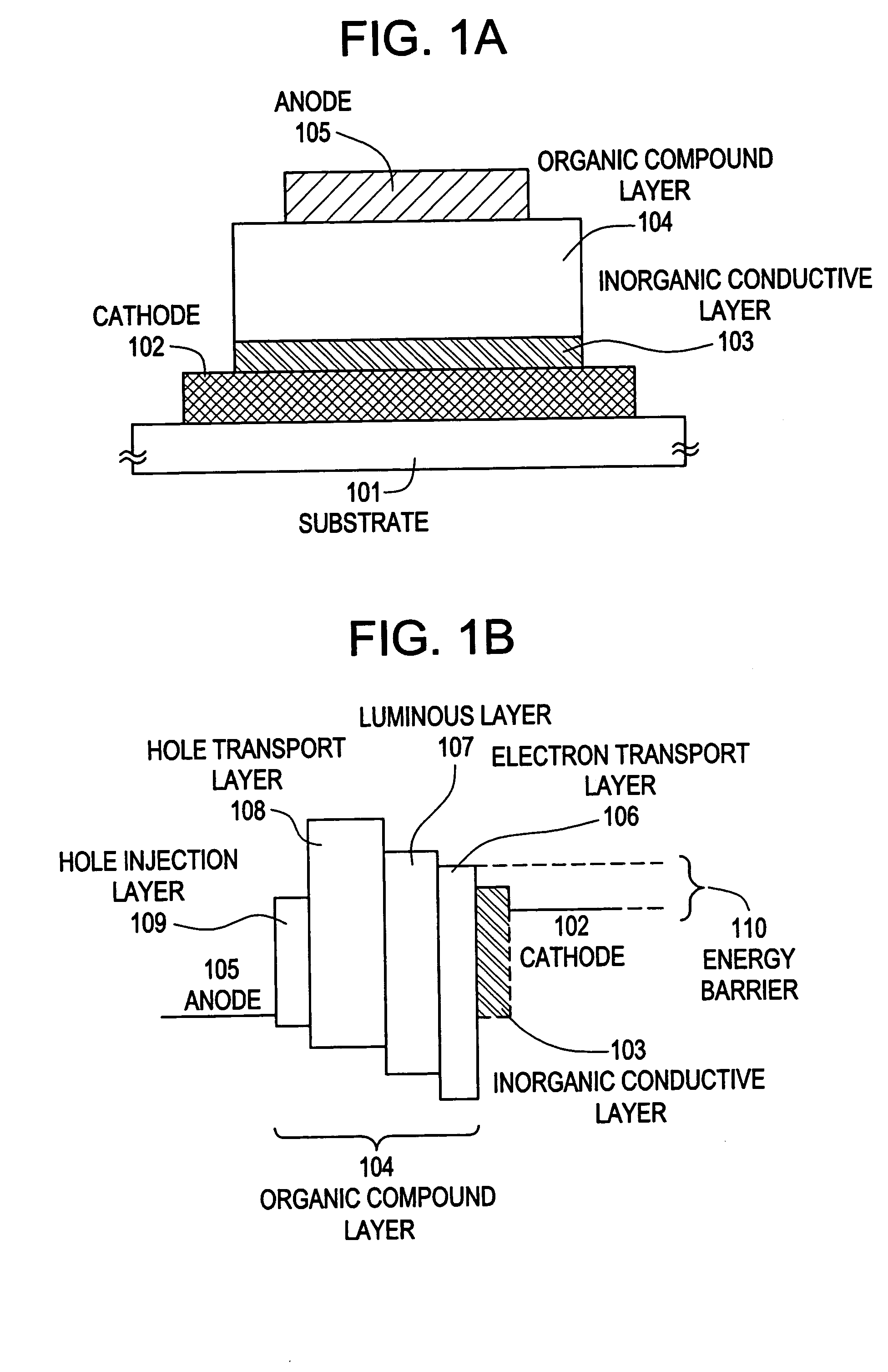
Luminous device
a luminous device and discharge tube technology, applied in the direction of discharge tube/lamp details, discharge tube luminescnet screens, other domestic articles, etc., can solve the problems of inability to easily generate noise, unnecessary backlight, and inability to drive luminous elements by dc voltage, so as to improve the capability of injecting electrons
- Summary
- Abstract
- Description
- Claims
- Application Information
AI Technical Summary
Benefits of technology
Problems solved by technology
Method used
Image

Examples
embodiment 1
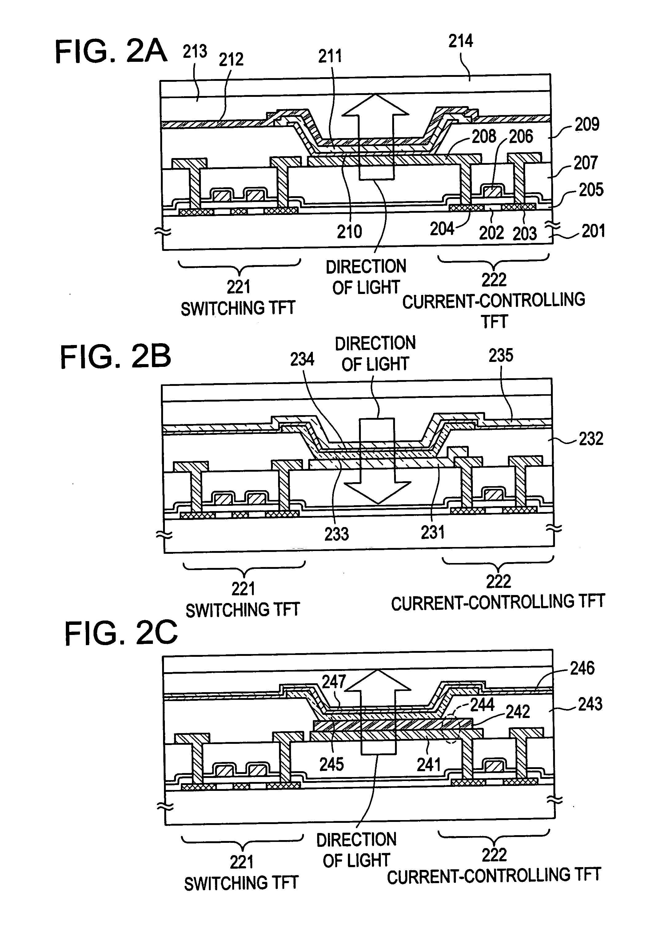
[0066] A sectional structure of a pixel section of a luminous device will be described as Embodiment 1 of the present invention, referring to FIG. 2A.
[0067] In FIG. 2A, semiconductor elements are formed on a substrate 201. As the substrate 201, a glass substrate having transparency is used. However, a quartz substrate may be used. As the semiconductor elements, TFTs are used. An active layer in each of the TFTs has at least a channel formed region 202, a source region 203 and a drain region 204.
[0068] The active layer in each of the TFTs is covered with a gate insulating film 205, and a gate electrode 206 overlapping the channel formed region 202 across the gate insulating film 205 is formed. An interlayer insulating film 207 covering the gate electrode 206 is deposited, and an electrode connected electrically to the source region or the drain region of each of the TFTs is formed on the interlayer insulating film 207. An electrode reaching a drain region 204 of a current-controlli...
embodiment 2
[0077] The following will describe a sectional structure of a pixel section of a luminous device as Embodiment 2 of the present invention, referring to FIG. 2B. The structure formed until the interlayer insulating film 207 is formed is the same as in Embodiment 1 except that the current-controlling TFT is formed to be of a p-channel type. Thus, detailed description thereof is omitted.
[0078] On the interlayer insulating film 207 is formed an electrode connected electrically to the source region or the drain region of each of the TFTs. An electrode reaching a drain region 204 of a current-controlling TFT 222, which is a p-channel type TFT, is connected electrically to an anode 231 of the luminous element. An insulating layer 232 having an opening which covers the edge portion of the anode 231 and has a tapered edge is deposited.
[0079] An organic compound layer 233 is deposited on the anode 231. An inorganic conductive layer 234 is deposited thereon. A cathode 235 is set up on the in...
embodiment 3
[0083] The following will describe a sectional structure of a pixel section of a luminous device as Embodiment 3 of the present invention, referring to FIG. 2C. The structure formed until the interlayer insulating film 207 is formed is the same as in Embodiment 1 except that the current-controlling TFT is formed to be of a p-channel type. Thus, detailed description thereof is omitted.
[0084] In the present Embodiment 3, a first electrode 241 is formed connected electrically to each TFT. A material for forming the first electrode 241 is preferably any one selected from conductive materials having light-shading property and a high reflectivity, for example, aluminum, titanium, or tungsten. It is preferred to use a monolayer made of any one selected from the above-mentioned conductive materials or a lamination wherein two or more selected from the conductive materials.
[0085] A second electrode 242 made of a material having a large work function is formed on the first electrode 241. It...
PUM
| Property | Measurement | Unit |
|---|---|---|
| electric conductivity | aaaaa | aaaaa |
| thickness | aaaaa | aaaaa |
| thickness | aaaaa | aaaaa |
Abstract
Description
Claims
Application Information
 - R&D
- Intellectual Property
- Life Sciences
- Materials
- Tech Scout
- Unparalleled Data Quality
- Higher Quality Content
- 60% Fewer Hallucinations
Browse by: Latest US Patents, China's latest patents, Technical Efficacy Thesaurus, Application Domain, Technology Topic, Popular Technical Reports.
© 2025 PatSnap. All rights reserved.Legal|Privacy policy|Modern Slavery Act Transparency Statement|Sitemap|About US| Contact US: help@patsnap.com