Method for Adjusting Metal Polishing Rate and Reducing Defects Arisen in a Polishing Process

a technology of metal polishing rate and polishing process, which is applied in the direction of grinding machines, manufacturing tools, lapping machines, etc., can solve the problems of increasing the demand for non-uniformity of the wafer surface, reducing the productivity of lithographs, and reducing the cost. , to achieve the effect of reducing the defects of dishing and erosion

Inactive Publication Date: 2012-11-01
SHANGHAI HUALI MICROELECTRONICS CORP
View PDF2 Cites 3 Cited by
  • Summary
  • Abstract
  • Description
  • Claims
  • Application Information

AI Technical Summary

Benefits of technology

[0011]The invention provides a method for adjusting metal polishing rate and reducing defects arisen in a polishing process, comprising steps of: adding an electric conduction system to a polishing apparatus in order to electrify a polishing fluid; and in the polishing process, making the polishing fluid flow through a polishing pad and a wafer to be polished, such that a polished metal surface of the wafer is electrically charged and thereby an oxidation of the polished metal surface of the wafer is controlled.
[0014]According to the aforementioned method for adjusting metal polishing rate and reducing defects arisen in a polishing process, the electric conduction system may provide a high potential to the polishing fluid, and the polished metal surface is at a higher potential in the polishing fluid, such that a reaction of the polished metal surface with chemical compositions in the polishing fluid is accelerated to generate metal oxide(s) or metal ion(s), and the accelerated oxidation reaction of the metal surface in turn results in an increased polishing rate, such that a scratch degree of the metal surface and a polishing pressure are reduced.
[0015]According to the aforementioned method for adjusting metal polishing rate and reducing defects arisen in a polishing process, the electric conduction system may provide a low potential to the polishing fluid, and the polished metal surface is at a lower potential in the polishing fluid. In such case, ions in the polishing fluid can suppress the reaction of the polished metal surface with the chemical compositions in the polishing fluid, so that the metal polishing rate is reduced and a more flat surface is thereby obtained.
[0016]The invention also provides an apparatus for adjusting metal polishing rate and reducing defects arisen in a polishing process, comprising a polishing stand, wherein the polishing stand is provided with an electric conduction system, and the electric conduction system has a voltage output terminal to contact the polishing fluid of the polishing stand.
[0018]To sum up, as the above technical solutions are introduced, the present invention has solved the problem that the dishing and erosion defects are prone to be formed in the existing polishing process, the potential of the polishing fluid is changed by means of the additionally arranged electric conduction system and thus the polishing rate of the polished metal is controlled, so as to achieve the object of reducing the dishing and erosion defects occurred in the polishing process.

Problems solved by technology

In the manufacture of wafers, as the upgrading of the process technology and the reduction of sizes of wires and grids, the lithograph technology has an increasing demand for non-uniformity of the wafer surface.
Referring to FIG. 1, which is a schematic structural diagram of a polishing stand according to the prior art, since the polishing rate is different for different mediums, defects of so-called dishing and erosion are often caused.
However, the pressure will have an impact on the polishing rate also, a low pressure corresponds to a lower polishing rate, which would not facilitate the improvement of productivity and the reduction of cost.
Obviously, the integrated circuit process requires a more accurate process control, and the metal polishing in the integrated circuit process is not suitable to be performed by using a single-directional / single-magnitude current or voltage.

Method used


Image

  • Method for Adjusting Metal Polishing Rate and Reducing Defects Arisen in a Polishing Process
  • Method for Adjusting Metal Polishing Rate and Reducing Defects Arisen in a Polishing Process
  • Method for Adjusting Metal Polishing Rate and Reducing Defects Arisen in a Polishing Process

Examples


Embodiment Construction

[0027]Hereinafter, the embodiments of the invention will be described in detail with reference to the appended drawings.

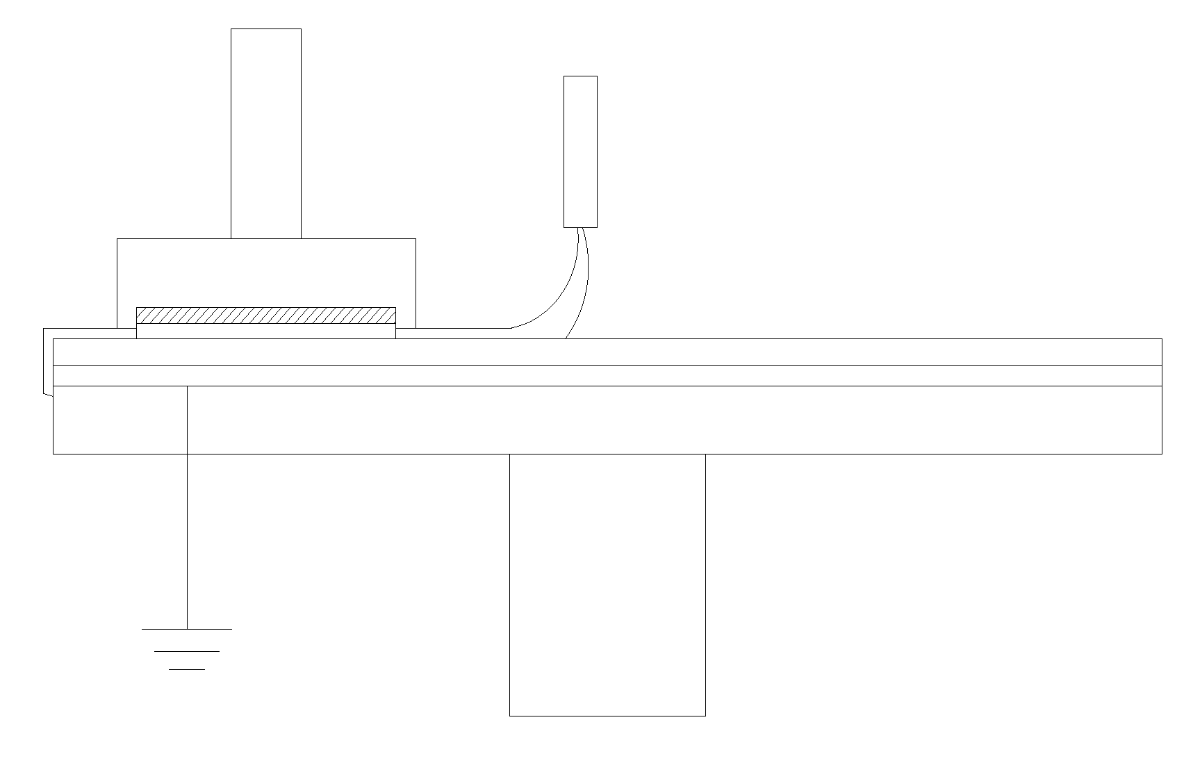
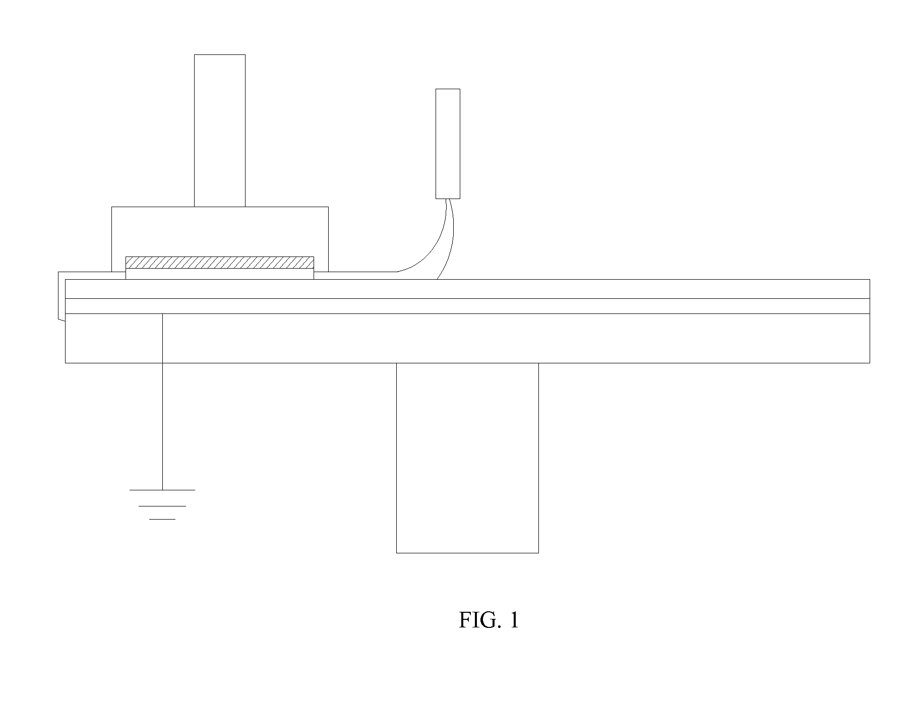
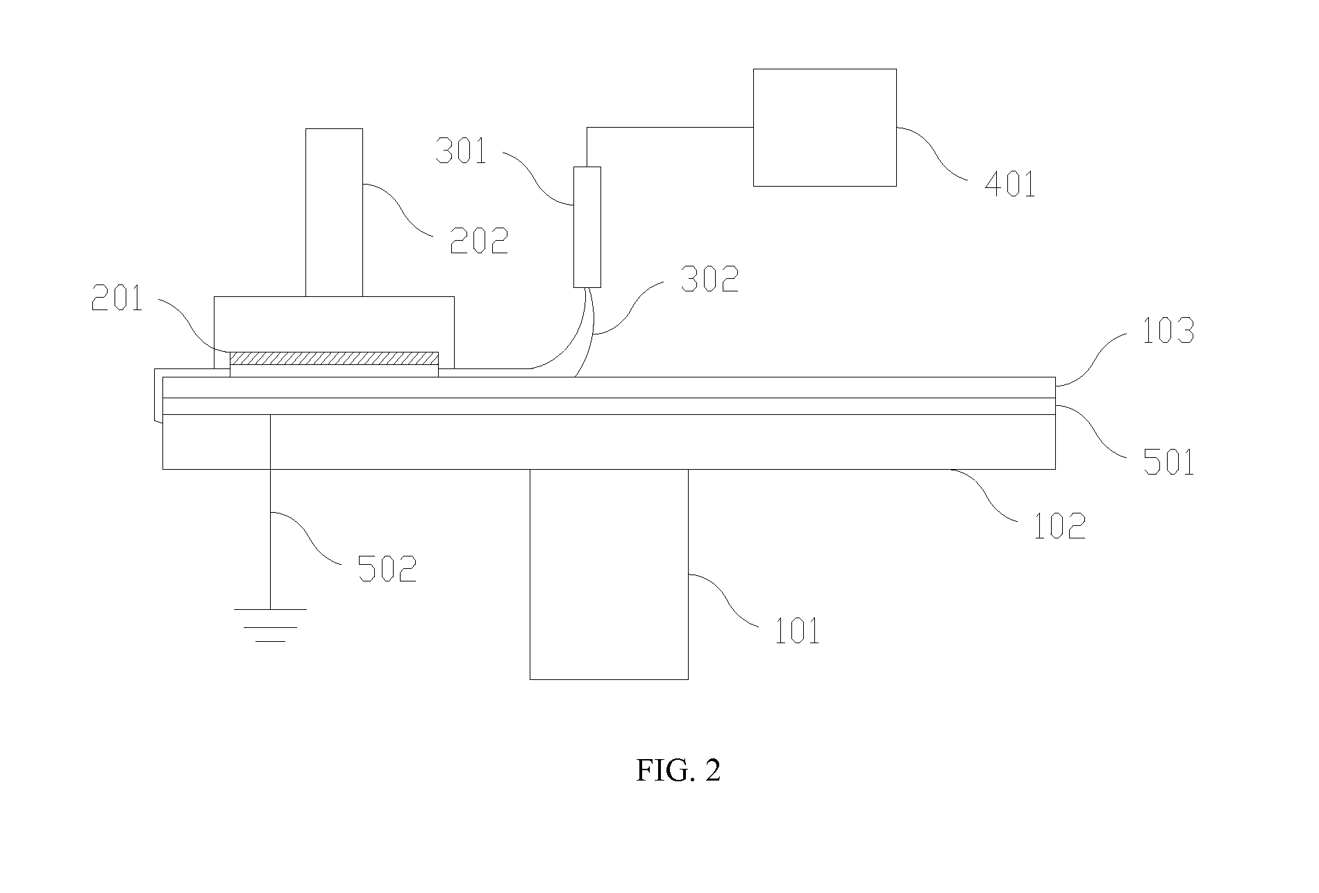
[0028]FIG. 2 is a schematic structural diagram of an apparatus for adjusting a metal polishing rate and reducing defects arisen in a polishing process according to the invention. Refer to FIG. 2, a method for adjusting a metal polishing rate and reducing defects arisen in a polishing process according to the invention may comprise a step of adding an electric conduction system 401 to the polishing apparatus. The electric conduction system 401 provides an additional current and electrical field, and is connected to a polishing fluid outlet 301 of a polishing stand of the polishing apparatus in order to electrify a polishing fluid 302 from the outlet 301. In the polishing process, the polishing fluid 302 flows down from the polishing fluid outlet 301, and flows through a polishing pad 103; a wafer 201 is mounted on a wafer bracket 202, and a surface of the wafer 201 ...


PUM

PropertyMeasurementUnit
Pressureaaaaaaaaaa

Abstract

The invention discloses a method for adjusting metal polishing rate and reducing defects arisen in a polishing process, in which a electric conduction system is additionally provided to a polishing apparatus to electrify the polishing fluid; in the polishing process, the polishing fluid flows through the polishing pad and the wafer to be polished, such that the polished metal surface of the wafer is electrically charged so as to control the oxidation of the polished metal surface of the wafer. The invention has solved the problem that the dishing and erosion defects are prone to be formed in the existing polishing process, the potential of the polishing fluid is changed by means of the additional electric conduction system and thus the polishing rate of the polished metal is controlled so as to reduce the dishing and erosion defects occurred in the polishing process.

Description

CROSS REFERENCE TO RELATED APPLICATIONS[0001]The present application is based upon and claims priority under 35 U.S.C. §119 to prior Chinese Patent Application No. 201110110366.0 filed on Apr. 29, 2011, the entire contents of which are incorporated herein by reference.TECHNICAL FIELD[0002]The present invention relates to a semiconductor metal polishing technique, and more particularly, to a method for adjusting metal polishing rate and reducing defects arisen in a polishing process.BACKGROUND[0003]In the manufacture of wafers, as the upgrading of the process technology and the reduction of sizes of wires and grids, the lithograph technology has an increasing demand for non-uniformity of the wafer surface. IBM developed and introduced CMOS products in 1985, and successfully applied CMOS in manufacturing 64 MB DRAM in 1990. CMP (Chemical Mechanical Planarization) has been developed rapidly since 1995 and is used widely in semiconductor industry.[0004]A polishing mechanism, taken coppe...

Claims


Application Information

Patent Timeline
IPC IPC(8): B24B1/00
CPCH01L21/7684H01L21/32125B24B37/24B24B37/22B24B37/046
Inventor ZHANG, SHOULONGBAI, YINGYINGCHEN, YUWEN
Owner SHANGHAI HUALI MICROELECTRONICS CORP
Why Eureka
Try Eureka