Photoconductive element
a photoconductive element and electromagnetic wave technology, applied in the direction of optical radiation measurement, instruments, spectrometry/spectrophotometry/monochromators, etc., can solve the problems of difficult the limit of the conventional photoconductive element to increase the resistivity of the photoconductive layer, etc., to increase the sensitivity of the entire element, increase the output, and increase the detection sensitivity
- Summary
- Abstract
- Description
- Claims
- Application Information
AI Technical Summary
Benefits of technology
Problems solved by technology
Method used
Image
Examples
first embodiment
[0022]With reference to FIGS. 1, 2A, 2B and 2C, the photoconductive element according to the first embodiment will be described. FIG. 1 is a sectional view of the photoconductive element according to present embodiment. FIGS. 2A, 2B and 2C are diagrams illustrating a correspondence between an element configuration and an equivalent circuit element.
[0023]The photoconductive element of the present embodiment includes a semiconductor layer 101 forming a photoconductive film, a semiconductor layer 102 stacked thereunder, and two electrodes 103 and 104 contacting the semiconductor layer 101. The semiconductor layer 101 is made of a semiconductor with a relatively high resistivity and for example, it has a relatively large band gap. In comparison with the semiconductor layer 101, the semiconductor layer 102 is made of a semiconductor with a relatively low resistivity and for example, it has a relatively small band gap. An equivalent circuit of the above structure when viewed from the surf...
second embodiment
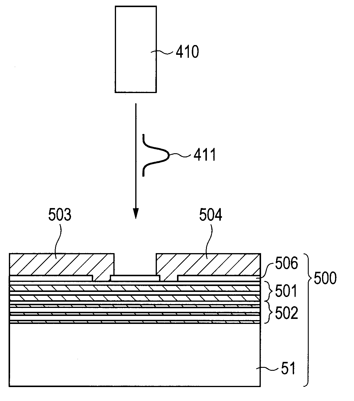
[0027]With reference to FIG. 3, the photoconductive element according to the second embodiment will be described. FIG. 3 is a sectional view of the photoconductive element, which is a variation of the first embodiment, according to the present embodiment. The present embodiment is different from the first embodiment in the configuration of a photoconductive film. Semiconductor superlattices 301 and 302 are used in the present embodiment. Note that electrodes 303 and 304 are the same as those in the first embodiment.
[0028]A semiconductor superlattice structure has been known as an artificial material obtained by repeating a pair of a quantum well with a thickness of about several nm and a tunneling barrier, and it can control an effective band gap of carriers and a macroscopic resistivity in a lateral direction. The effective band gap can be evaluated by the energy difference from the bottom of an electron miniband in the conduction band to the top of a hole miniband in the valence b...
first example
[0031]With reference to FIGS. 4A and 4B, a specific electromagnetic wave generating / detecting apparatus according to the first example will be described. FIG. 4A is a sectional view illustrating a configuration of the electromagnetic wave generating / detecting apparatus and the photoconductive element according to the present example. FIG. 4B is a top view illustrating a configuration of the photoconductive element.
[0032]In the present example, the photoconductive film includes an LT-InGaAsP layer 401 and an LT-InGaAs layer 402. These layers are formed by crystal growth on a semi-insulating InP substrate 41. The prefix “LT-” refers to a low-temperature growth method for use in the crystal growth. For example, an molecular beam epitaxy (MBE) method is used to perform crystal growth at a temperature of about 250° C. The LT-InGaAsP layer 401 has a band gap corresponding to 1.5 μm; and the LT-InGaAs layer 402 has a band gap corresponding to 1.67 μm. In the present example, each thickness...
PUM
 Abstract
Description
Claims
Application Information
 - R&D
- Intellectual Property
- Life Sciences
- Materials
- Tech Scout
- Unparalleled Data Quality
- Higher Quality Content
- 60% Fewer Hallucinations
Browse by: Latest US Patents, China's latest patents, Technical Efficacy Thesaurus, Application Domain, Technology Topic, Popular Technical Reports.
© 2025 PatSnap. All rights reserved.Legal|Privacy policy|Modern Slavery Act Transparency Statement|Sitemap|About US| Contact US: help@patsnap.com


