
Method of circuit layout by photosensitive environment-friendly ink

Inactive Publication Date: 2012-09-06
TAIWAN NANOTECH CORP
View PDF1 Cites 2 Cited by
  • Summary
  • Abstract
  • Description
  • Claims
  • Application Information

AI Technical Summary

Benefits of technology

[0007]Comparing to the conventional technology, the present invention provides a method of circuit layout by photosensitive environment-friendly ink, which is capable of reducing the complicated steps in the pre-manufacturing process of the printed circuit board including pre-made mask sheets, coating copper foils, exposure and developing. In other words, the present invention utilizes inkjet controlling technology to inject the perform photosensitive environment-friendly ink through the nozzle to generate layout on specific areas on the printed circuit board having a copper foil layer to form the circuit layout pattern, thus producing the printed circuit board with the circuit layout pattern. Referring to the surface of the printed circuit board, the manufacturing process is similar to the printing process of a document. Furthermore, the ink of the invention has the characteristics of being environment-friendly, safe for storage, suited to hard base materials such as printed circuit boards, wear proof, chemical proof, heat resistance, quick drying, low ink bleeding, and high resolution.

Problems solved by technology

However, with the reduced size and precision of electronic products, the PCB manufacturing process also requires reduced size and precision.

Method used


Image

  • Method of circuit layout by photosensitive environment-friendly ink

Examples


Embodiment Construction

[0009]The techniques employed by the present invention to achieve the foregoing objectives, characteristics and effects thereof are described hereinafter by way of examples with reference to the accompanying drawings.

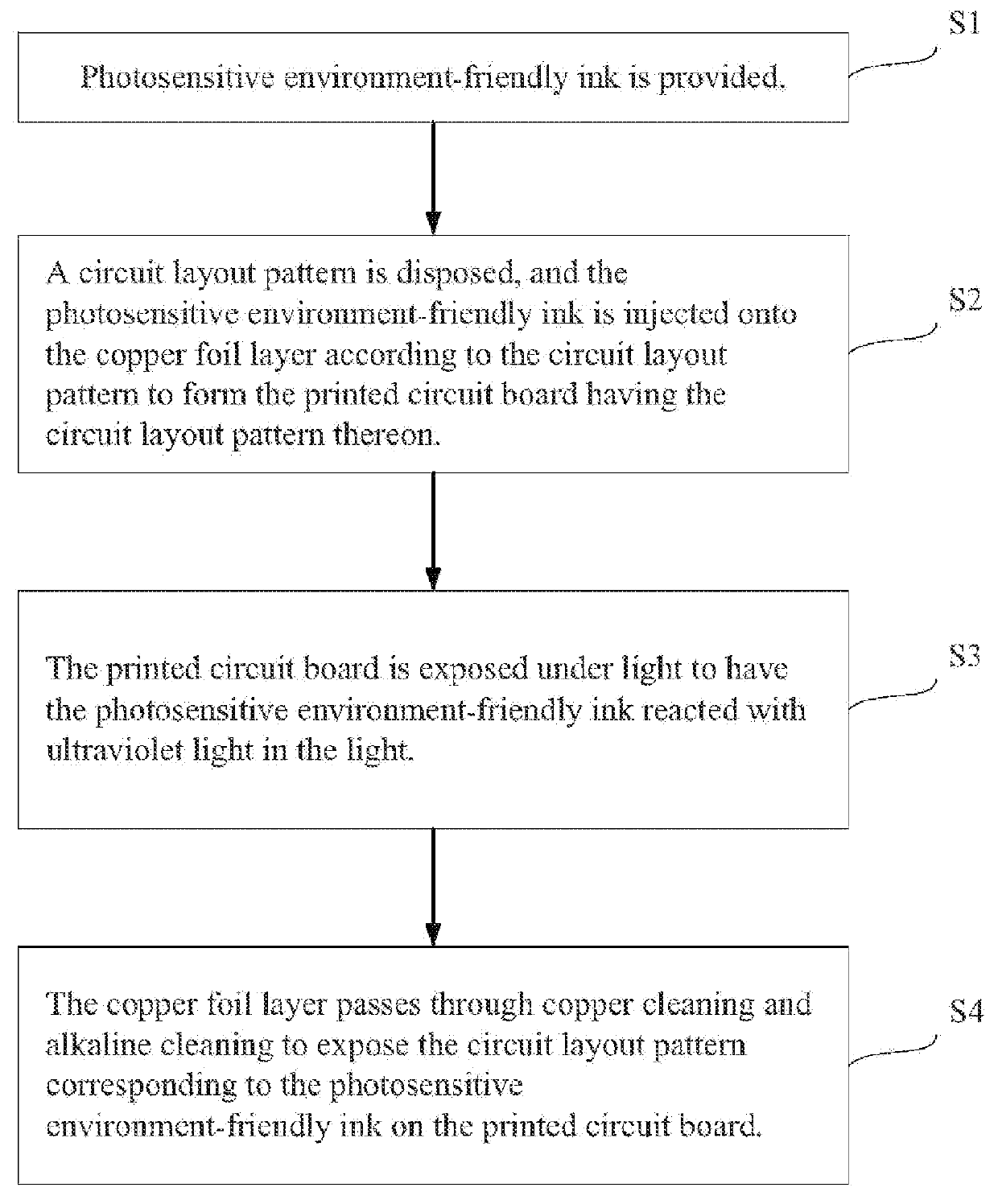
[0010]Referring to FIG. 1, which shows a flow chart of an embodiment of the method of circuit layout by photosensitive environment-friendly ink of the present invention. In FIG. 1, the method of circuit layout by photosensitive environment-friendly ink is used in a printed circuit board having a copper foil layer. The steps comprises: in step S1, photosensitive environment-friendly ink is provided. In step S2, a circuit layout pattern is disposed, and the photosensitive environment-friendly ink is injected onto the copper foil layer according to the circuit layout pattern to form the printed circuit board having the circuit layout pattern thereon. In step S3, the printed circuit board is exposed under light to have the photosensitive environment-friendly ink reacted wit...


PUM

PropertyMeasurementUnit
Sizeaaaaaaaaaa
Sizeaaaaaaaaaa
Sizeaaaaaaaaaa

Abstract

A method of circuit layout by photosensitive environment-friendly ink, which is used in a printed circuit board having a copper foil layer. The method comprises: providing photosensitive environment-friendly ink; disposing a circuit layout pattern, and injecting the photosensitive environment-friendly ink on the copper foil layer according to the circuit layout pattern to form the printed circuit board having the circuit layout pattern thereon; exposing the printed circuit board under light to have the photosensitive environment-friendly ink reacted with ultraviolet light in the light; and copper cleaning and alkaline cleaning the copper foil layer to expose the circuit layout pattern corresponding to the photosensitive environment-friendly ink on the printed circuit board. The invention can be used to achieve reducing steps in the conventional printed circuit board manufacturing process, reduced usage of chemical materials, simplified transfer of manufacturing process, optimization of wirings in the circuit layout, and low cost manufacture.

Description

FIELD OF THE INVENTION[0001]The present invention relates to a method of circuit layout by photosensitive environment-friendly ink, and particularly to a method of providing circuit layout on a printed circuit board using photosensitive environment-friendly ink.BACKGROUND[0002]In conventional technology, a printed circuit board (PCB) is a circuit board with its circuitry pattern being produced by a printing process. With the enhanced requirement of the wiring resolution of the layout on the printed circuit board, there is a need to improve the conventional manufacturing process of the printed circuit board. Nowadays most printed circuit boards are manufactured by pressing film or coating of etching resist, passing through the exposure and developing processes, performing etching to remove the exposed copper foils and to form the wirings, and then washing and removing the etching resist to finish the manufacturing process. However, with the reduced size and precision of electronic pr...

Claims


Application Information

Patent Timeline
IPC IPC(8): H05K3/10
CPCH05K3/064Y10T29/49155H05K2203/013
Inventor HSIEH, CHENG YANGLIANG, CHENG LIN
Owner TAIWAN NANOTECH CORP
Learn More