Semiconductor device and method for manufacturing the same

a semiconductor and manufacturing method technology, applied in the direction of semiconductor devices, basic electric elements, electrical appliances, etc., can solve the problems of low performance of semiconductor devices, and achieve the effects of low semiconductor device performance, high crystallinity, and high bonding characteristi

Active Publication Date: 2012-08-16
SUMITOMO ELECTRIC IND LTD
View PDF1 Cites 13 Cited by
  • Summary
  • Abstract
  • Description
  • Claims
  • Application Information

AI Technical Summary

Benefits of technology

[0008]Further, according to the method disclosed in PTL 2, since the etching stop layer having unique characteristics is interposed between the underlying layer and the semiconductor layer, crystallinity of n type GaN layer, active layer and p type GaN layer to be grown on the semiconductor layer lowers, resulting in lower performance of the semiconductor device.
[0009]It is an object of the present invention to solve the above-described problem and to provide an n-down type semiconductor device having a semiconductor layer of high crystallinity and high bonding characteristic to a supporting substrate.
[0015]By the present invention, an n-down type semiconductor device having a semiconductor layer of high crystallinity and high bonding characteristic to a supporting substrate can be provided.

Problems solved by technology

Since it is difficult to bond the supporting substrate to the n type semiconductor layer having a rough surface, it is difficult by the methods disclosed in PTLs 1 to 3 to manufacture a n-down type semiconductor device in which an n type semiconductor layer is bonded to a supporting substrate.
Further, according to the method disclosed in PTL 2, since the etching stop layer having unique characteristics is interposed between the underlying layer and the semiconductor layer, crystallinity of n type GaN layer, active layer and p type GaN layer to be grown on the semiconductor layer lowers, resulting in lower performance of the semiconductor device.

Method used


Image

  • Semiconductor device and method for manufacturing the same
  • Semiconductor device and method for manufacturing the same
  • Semiconductor device and method for manufacturing the same

Examples


embodiment 1

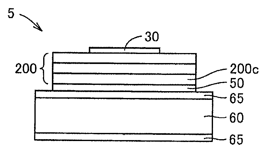
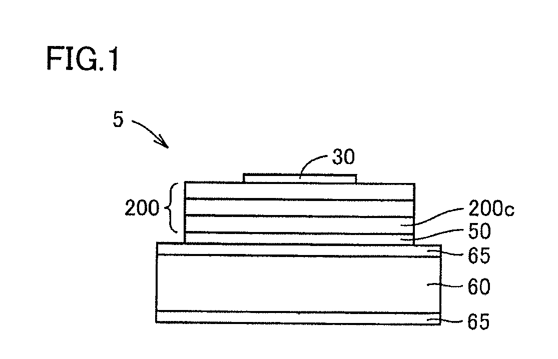
[0027]Referring to FIG. 1, a semiconductor device 5 in accordance with an embodiment of the present invention includes a supporting substrate 60, a conductive layer 50 placed on supporting substrate 60, and at least one group III nitride semiconductor layer 200 placed on conductive layer 50, and among the group III nitride semiconductor layers 200, a conductive-layer-neighboring group III nitride semiconductor layer 200c adjacent to conductive layer 50 has n type conductivity, dislocation density of at most 1×107 cm−2, and oxygen concentration of at most 5×1018 cm−3.

[0028]Semiconductor device 5 in accordance with the present embodiment is an n-down type semiconductor device, since the conductive-layer-neighboring group III semiconductor layer 200c is of n type conductivity, and since it has dislocation density of at most 1×107 cm−2 and oxygen concentration of at most 5×1018 cm−3, group III nitride semiconductor layer 200 including such conductive-layer-neighboring group III semicond...

embodiment 2

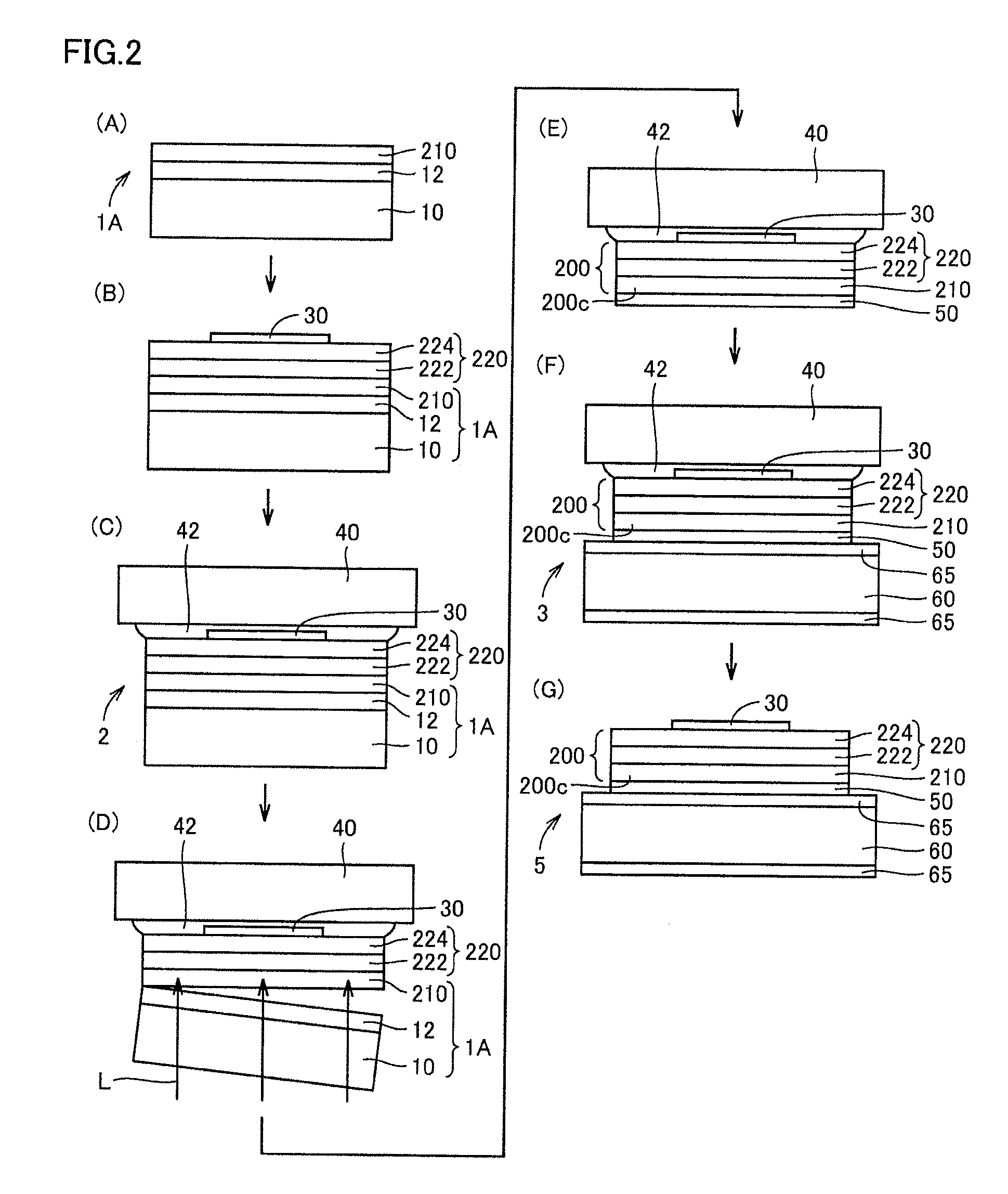
[0037]Referring to FIGS. 2, 3 and 6, the method of manufacturing a semiconductor device 5 in accordance with another embodiment of the present invention includes the steps of: preparing a first composite substrate 1A, 1B having a first group III nitride semiconductor layer 210 joined to an underlying substrate 10 ((A) in FIGS. 2, 3 and 6); growing at least one second group III nitride semiconductor layer 220 on the first group III nitride semiconductor layer 210 of the first composite substrate 1A, 1B ((B) in FIGS. 2,3 and 6); forming a second composite substrate 2 by joining a temporary supporting substrate 40 to the second group III nitride semiconductor layer 220 ((C) of FIGS. 2, 3 and 6); removing underlying substrate 10 from the second composite substrate 2 ((D) of FIGS. 2, 3 and 6); forming conductive layer 50 on the first group III nitride semiconductor layer 210 ((E) in FIG. 2, (F) in FIGS. 3 and 6); forming a third composite substrate 3 by joining supporting substrate 60 to...

embodiment 3

[0072]Referring to FIGS. 4 and 5, the method of manufacturing a semiconductor device in accordance with a still further embodiment of the present invention includes the steps of: preparing the first composite substrate 1B having the first group III nitride semiconductor layer 210 joined to underlying substrate 10 ((A) in FIGS. 4 and 5); growing at least one second group III nitride semiconductor layer 220 on the first group III nitride semiconductor layer 210 of the first composite substrate 1B ((B) in FIGS. 4 and 5); joining temporary supporting substrate 40 to the second group III nitride semiconductor layer 220 to form the second composite substrate 2 ((C) in FIGS. 4 and 5); removing underlying substrate 10 from the second composite substrate 2 ((D) in FIGS. 4 and 5); removing the first group III nitride semiconductor layer 210 ((F) in FIGS. 4 and 5); forming conductive layer 50 on the second group III nitride semiconductor layer 220 ((G) in FIGS. 4 and 5); joining supporting sub...


PUM

PropertyMeasurementUnit
wavelengthaaaaaaaaaa
thicknessaaaaaaaaaa

Abstract

A semiconductor device includes a supporting substrate, a conductive layer placed on the supporting substrate, and at least one group III nitride semiconductor layer placed on the conductive layer. Of the group III nitride semiconductor layers, a conductive-layer-neighboring group III nitride semiconductor layer has n type conductivity, dislocation density of at most 1×107 cm−2, and oxygen concentration of at most 5×1018 cm−3. Thus, an n-down type device having a semiconductor layer of high crystallinity can be provided.

Description

BACKGROUND OF THE INVENTION[0001]1. Field of the Invention[0002]The present invention relates to a semiconductor device and manufacturing method thereof and, more specifically, to a vertical semiconductor device having superior characteristics and to a method of manufacturing the same. Description of the[0003]2. Background ArtVertical semiconductor devices, including both light emitting devices and electronic devices, have characteristics that packaging is easy and area efficiency is high. As a method of manufacturing a vertical semiconductor device having such characteristics, a method of joining semiconductor layers grown on an underlying substrate to a supporting substrate different from the underlying substrate has been proposed.[0004]By way of example, Japanese Patent Laying-Open No. 2010-212719 (PTL 1) discloses forming rugged patterns on a surface of a semiconductor layer (a surface of an n type semiconductor layer) after removing an underlying substrate from semiconductor la...

Claims


Application Information

Patent Timeline
Patent Type & Authority Applications(United States)
IPC IPC(8): H01L29/20H01L21/762
CPCH01L33/007H01L33/025H01L33/0079H01L33/0093H01L33/32
Inventor KYONO, TAKASHIISHIHARA, KUNIAKIHACHIGO, AKIHIROYOSHIDA, TAKAHISAUENO, MASAKIKIYAMA, MAKOTO
Owner SUMITOMO ELECTRIC IND LTD
Why Eureka
Try Eureka