Solvent annealing block copolymers on patterned substrates
a technology of block copolymer and substrate, applied in the field of nanofabrication techniques, can solve the problems of limited features of traditional patterning methods such as photolithography and electron beam lithography that have emerged from the microelectronics industry, and achieve the effects of improving dimensional control of features, improving line edge and line width roughness, and high pattern perfection
- Summary
- Abstract
- Description
- Claims
- Application Information
AI Technical Summary
Benefits of technology
Problems solved by technology
Method used
Image
Examples
example 1
Effect of Solvent Choice on BCP Film Morphology and Period
[0082]30-nm-thick films of PS-b-P2VP (40k-b-40k) were coated on homogeneous substrates grafted by a series of PS-r-P2VP-r-PHEMA containing 41.8%-67.6% styrene and then annealed in acetone, N,N-dimethylformamide (DMF), toluene, carbon disulfide (CS2), and methanol for 16 h, 2 h, 9 h, 20 h, and 16 h respectively. 200-nm-thick films of PS-b-P2VP (40k-b-40k) on PS60.8%-r-P2VP-r-PHEMA brush were annealed in DMF and acetone for cross-sectional SEM imaging. PS-b-P2VP (40k-b-40k) thin films showed various morphologies and periods after being annealed in different solvent vapors.
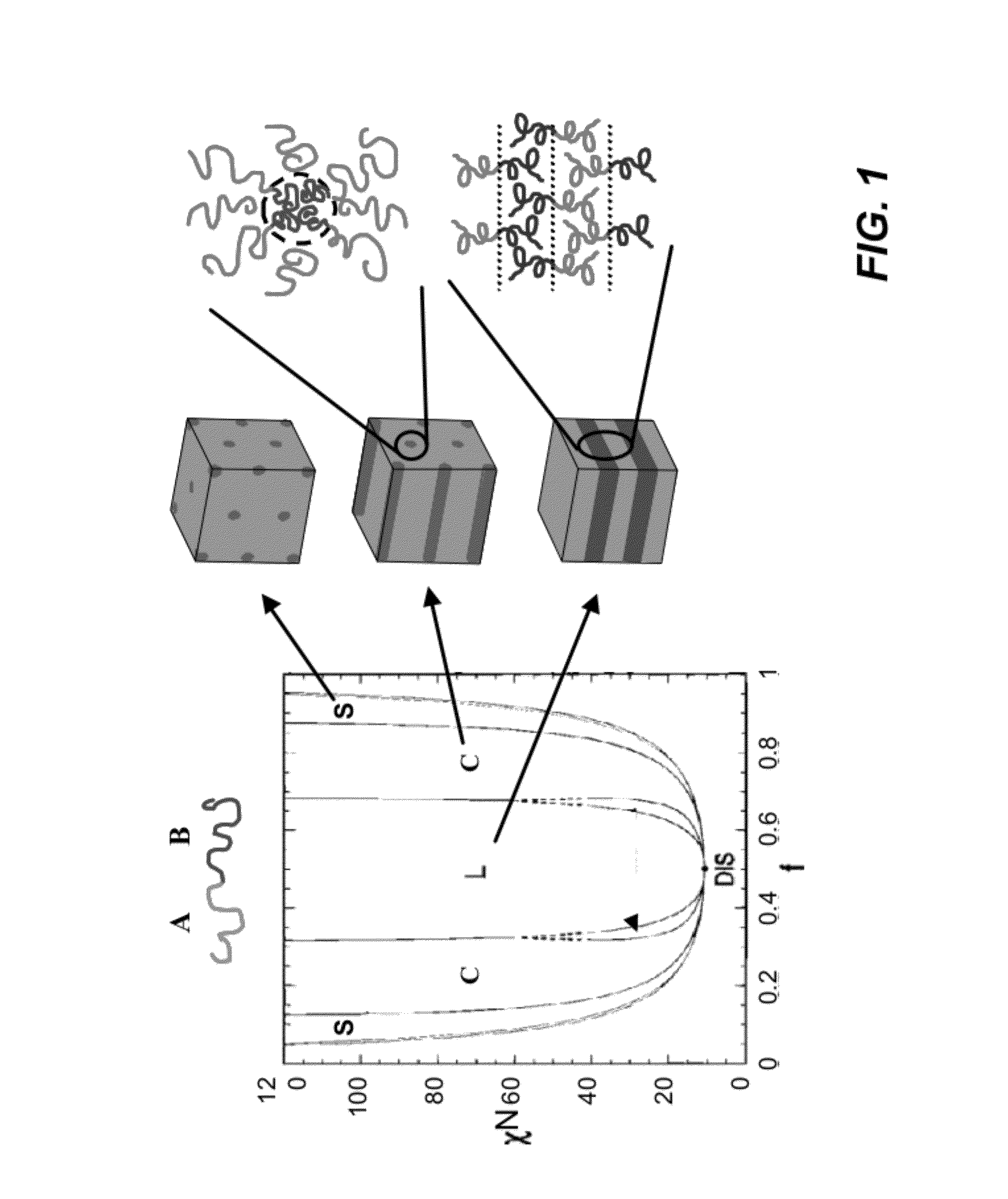
[0083]PS-b-P2VP was chosen as an illustrative system since it is difficult for thermal annealing due to the large difference in surface tensions between PS and P2VP blocks, and it has relatively high Flory-Huggins interaction parameter (x of about 0.217 at 20° C.).
[0084]Only micellar structure was observed on films annealed in methanol vapor. Toluene and CS2 v...
example 2
Chemical Patterning of and Solvent Annealing-Induced Directed Assembly on 1:1 and 1:n Patterns
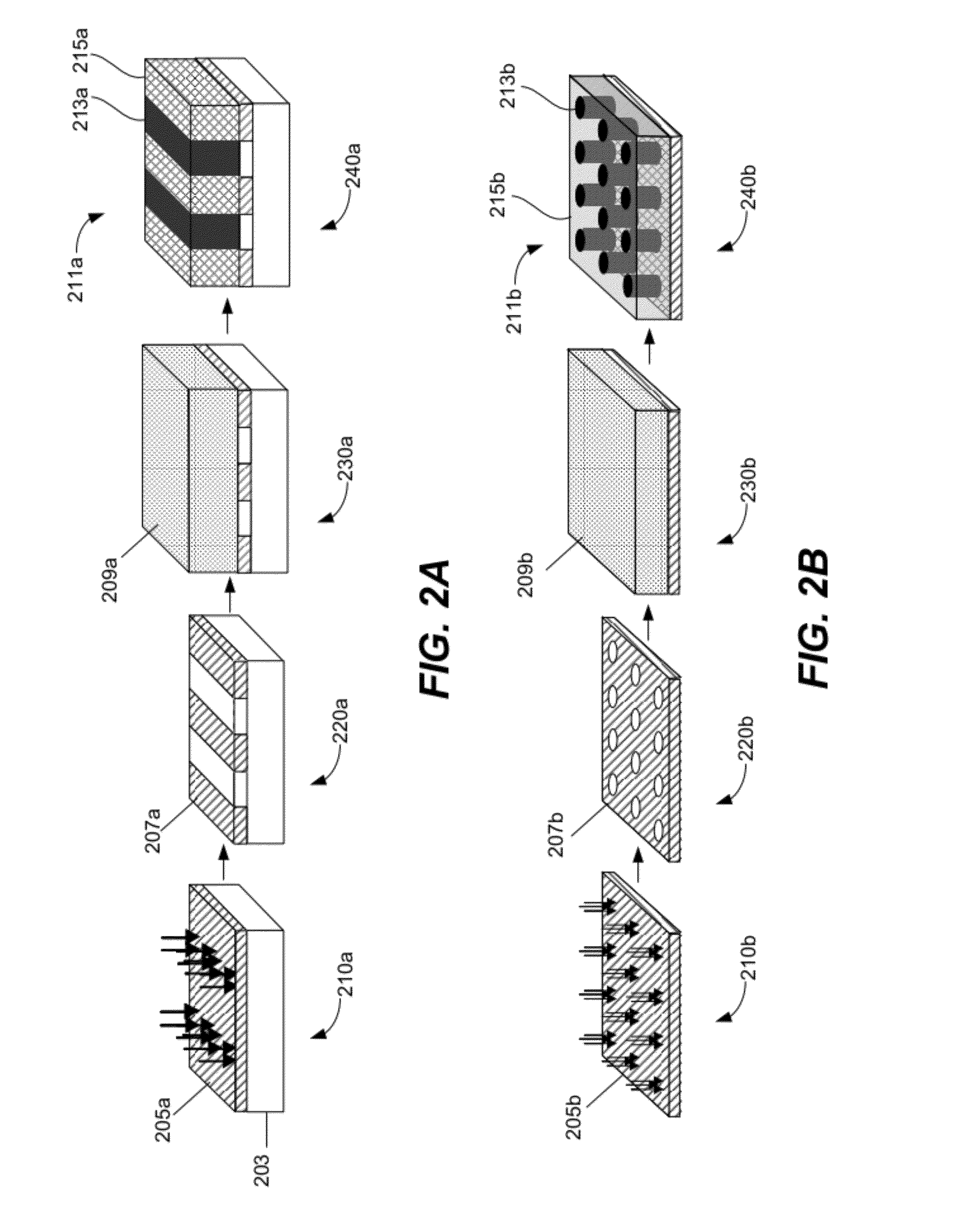
[0088]FIG. 12 is an example of a schematic illustration of processes used to create lithographically defined chemical patterns and subsequent solvent-vapor-induced directed assembly of BCP thin films. The preparation of 1:1 chemical patterns with Ls approximately equals to the period of the vitrified BCP domains Lv started with grafting PS—OH brush on silicon substrates. Then a layer of PMMA photoresist was applied and patterned with extreme ultraviolet interference lithography (EUV-IL). The chemical patterns were obtained by exposing the photoresist patterns to an O2 plasma and stripping the remaining photoresist in chlorobenzene. The chemical patterns with Ls approximately equal to nLv (n=2, 3, 4) were created on silicon substrates deposited with a thin layer of crosslinked PS (XPS) mats. A layer of PMMA photoresist was applied on the XPS mats with used EUV-IL and e-beam lithography to ob...
example 3
Directed Assembly of PS-b-PMMA Films by Solvent Annealing
Materials and Methods
[0098]Materials: PS-b-PMMA (Mn=52-52 and 95-92 kg / mol, polydispersity index (PDI)=1.10 and 1.06 respectively, Lo 50 nm and 80 nm, respectively), hydroxyl terminated PS (PS—OH, Mn=6.0 kg / mol, PDI=1.07), and hydroxyl terminated PMMA (PMMA-OH, Mn=6.3 kg / mol, PDI=1.06) were purchased from Polymer Source Inc. PMMA photoresist (Mn=950 kg / mol, 4 wt % in chlorobenzene) was purchased from MicroChem Inc. All solvents were purchased from Aldrich and used as received. Hydroxyl terminated poly(styrene-r-methyl methacrylate) (PS-r-PMMA-OH, Mn=12.5 kg / mol, PDI=1.25) was synthesized by nitroxide-mediated polymerization. The styrene fraction was determined to be 57 mol % by 1H NMR analysis. Crosslinkable PS (Mn=30.5 kg / mol, PDI=1.22) was synthesized by nitroxide-mediated copolymerization of styrene and glycidyl methacrylate and contained about 4 mol % of crosslinkable epoxy groups.
[0099]Substrate modification: 1 wt % tolue...
PUM
| Property | Measurement | Unit |
|---|---|---|
| Temperature | aaaaa | aaaaa |
| Thickness | aaaaa | aaaaa |
| Structure | aaaaa | aaaaa |
Abstract
Description
Claims
Application Information
 - R&D
- Intellectual Property
- Life Sciences
- Materials
- Tech Scout
- Unparalleled Data Quality
- Higher Quality Content
- 60% Fewer Hallucinations
Browse by: Latest US Patents, China's latest patents, Technical Efficacy Thesaurus, Application Domain, Technology Topic, Popular Technical Reports.
© 2025 PatSnap. All rights reserved.Legal|Privacy policy|Modern Slavery Act Transparency Statement|Sitemap|About US| Contact US: help@patsnap.com


