
Differential plate line screen test for ferroelectric latch circuits

a ferroelectric latch and plate line technology, applied in the field of semiconductor integrated circuits, can solve the problems of essentially volatile devices, recall is thus a general destructive read, and conventional mos capacitors lose their stored charge, so as to achieve accurate and efficient screening

Active Publication Date: 2012-08-02
TEXAS INSTR INC
View PDF5 Cites 7 Cited by
  • Summary
  • Abstract
  • Description
  • Claims
  • Application Information

AI Technical Summary

Benefits of technology

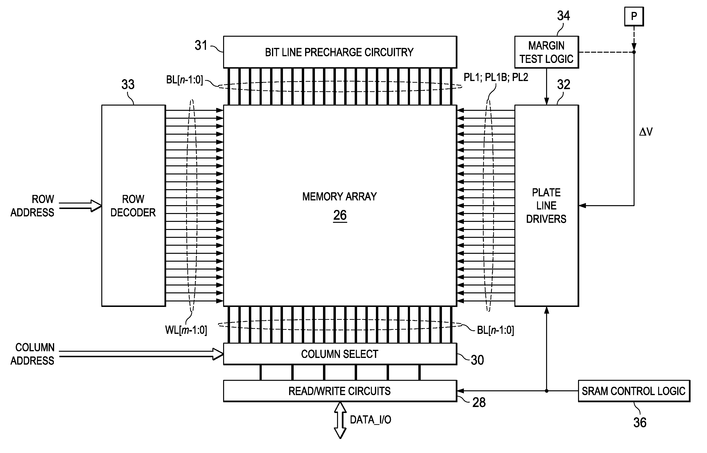
This patent describes a method and circuit for screening non-volatile circuits, such as memory cells and logic elements, for their stability over time and usage. The method accurately reflects the behavior of the circuits and can characterize populations of circuits with ferroelectric elements. The circuit includes a latch circuit with two storage nodes, in which ferroelectric capacitors are coupled to each of the storage nodes. The method involves performing a restore operation with a reduced voltage to determine the stability of the circuit, and then subjecting the circuits to accelerated stress, such as a bake operation, and testing their restore capability. The results of the testing operation are used to select a reduced voltage level for screening manufactured circuits to remove potential reliability risks.

Problems solved by technology

As is fundamental in the art, however, those devices are essentially volatile, in that logic and memory circuits constructed according to these technologies do not retain their data states upon removal of bias power.
In contrast, conventional MOS capacitors lose their stored charge on power-down of the device.
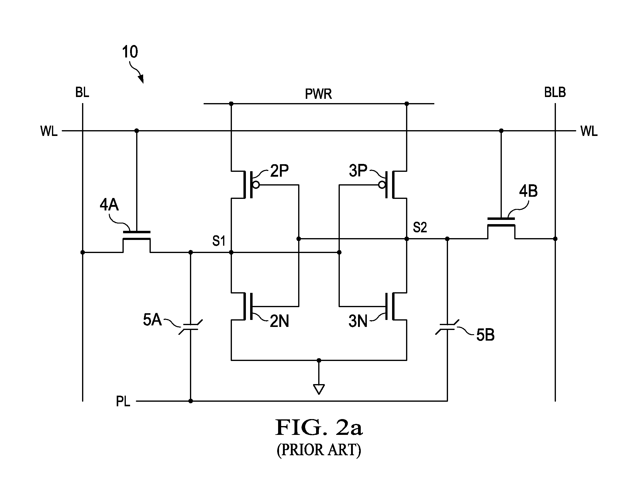
The polarization state of capacitor 5B is destroyed in this recall (or “restore”) operation; this recall is thus a generally destructive read.
As before, this restore operation is destructive of the programmed state, requiring reprogramming of capacitors 5A, 5B, 7A, 7B when appropriate.
However, ferroelectric elements such as capacitors are known to be vulnerable to later-life degradation due to various effects.
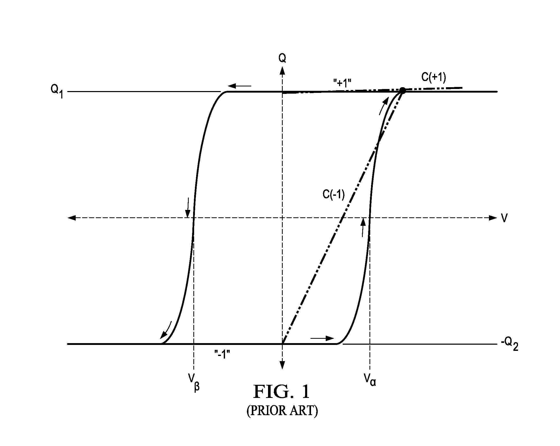
Repeated read / write cycles (i.e., polarization and destructive read operations) can degrade the polarizability of ferroelectric capacitors, as can the effects of time and temperature.
In this somewhat extreme case, the effects of imprint include inadequate polarization of the capacitor in either state, as well as poorly defined coercive voltages.
As evident from FIG. 3, severe imprint greatly reduces the ability to distinguish the two polarization states from one another.
Because the restore or recall operation relies on differences in capacitance between the two states, this weakness in polarization increases the likelihood that device imbalances, or noise events, can cause the memory cell or logic element incorporating ferroelectric capacitors to fall victim to a data error on restoring a programmed state.
Certainly the likelihood of such errors increases as degradation of the ferroelectric material over time, temperature, and usage occurs.
Such data errors have been observed in modern high-performance integrated circuits incorporating ferroelectric capacitors for non-volatile data and logic state retention.
Of course, in circuit implementations such as memory cells and logic circuits, it is difficult if not impossible to obtain a direct measurement of the polarization characteristics of each embedded ferroelectric capacitor.
However, it has been observed that there is a poor correlation between those devices failing such a reduced Vdd storage test, and those devices that exhibit the weakest reliability due to time-dependent polarization degradation, especially as reliability requirements continue to become more stringent.
That approach is somewhat cumbersome insofar as construction of write circuits in the memories is concerned.
In addition, this bit line disturb voltage approach is not applicable to logic circuits such as flip-flop 16 that do not have accessible “bit lines” at all, especially for such circuits that are embedded in complex logic chains and data paths.

Method used


Image

  • Differential plate line screen test for ferroelectric latch circuits
  • Differential plate line screen test for ferroelectric latch circuits
  • Differential plate line screen test for ferroelectric latch circuits

Examples


Embodiment Construction

[0045]This invention will be described in connection with certain of its embodiments, namely as implemented into non-volatile latch circuits implemented into memory resources in the form of static random access memory (SRAM) or as bistable multivibrators (flip-flops), because it is contemplated that this invention is especially beneficial when applied to such circuits. However, it is also contemplated that other logic and memory circuits may also greatly benefit from this invention. Accordingly, it is to be understood that the following description is provided by way of example only, and is not intended to limit the true scope of this invention as claimed.

[0046]As mentioned above, this invention is suitable for use in connection with semiconductor memory circuits, whether serving as a stand-alone integrated circuit or as embedded into larger scale integrated circuits such as microprocessors, microcontrollers, or the so-called “system on a chip” (SoC) integrated circuits. This invent...


PUM


Abstract

Non-volatile latch circuits, such as in memory cells and flip-flops, that are constructed for reliability screening. The non-volatile latch circuits each include ferroelectric capacitors coupled to storage nodes, for example at the outputs of cross-coupled inverters. Separate plate lines are connected to the ferroelectric capacitors of the complementary storage nodes. A time-zero test of the latch stability margin is performed by setting a logic state at the storage nodes, then programming the state into the ferroelectric capacitors by polarization. After power-down, the plate lines are biased with a differential voltage relative to one another, and the latch is then powered up to attempt recall of the programmed state. The differential voltage disturbs the recall, and provides a measure of the cell margin and its later-life reliability.

Description

CROSS-REFERENCE TO RELATED APPLICATIONS[0001]This application is a divisional of U.S. application Ser. No. 12 / 781,601, filed May 17, 2010, which claims priority, under 35 U.S.C. §119(e), to Provisional Application No. 61 / 180,322, filed May 21, 2009, the contents of both are herein incorporated by reference.STATEMENT REGARDING FEDERALLY SPONSORED RESEARCH OR DEVELOPMENT[0002]Not applicable.BACKGROUND OF THE INVENTION[0003]This invention is in the field of semiconductor integrated circuits. Embodiments of this invention are more specifically directed to reliability screening of non-volatile storage elements in such integrated circuits.[0004]Conventional metal-oxide-semiconductor (MOS) and complementary MOS (CMOS) logic and memory devices are prevalent in modern electronic devices and systems, as they provide an excellent combination of fast switching times and low power dissipation, along with their high density and suitability for large-scale integration. As is fundamental in the art...

Claims


Application Information

Patent Timeline
Patent Type & Authority Applications(United States)
IPC IPC(8): G11C11/22
CPCG11C29/50G11C11/22
Inventor SUMMERFELT, SCOTT R.RODRIGUEZ, JOHN ANTHONYMCADAMS, HUGH P.BARTLING, STEVEN CRAIG
Owner TEXAS INSTR INC
Learn More