Voltage characteristic regulating method of latch circuit, voltage characteristic regulating method of semiconductor device, and voltage characteristic regulator of latch circuit

a voltage characteristic and latch circuit technology, applied in the direction of digital storage, process and machine control, instruments, etc., can solve the problems of a long time and malfunction of the latch circuit, and achieve the effect of reducing current, low threshold voltage, and rising threshold voltag

Inactive Publication Date: 2012-07-19
SEMICON TECH ACADEMIC RES CENT
View PDF13 Cites 5 Cited by
  • Summary
  • Abstract
  • Description
  • Claims
  • Application Information

AI Technical Summary

Benefits of technology

[0009]In one preferable application of the voltage characteristic regulating method of the latch circuit according to the above aspect of the invention, preset low voltage that is lower than power-supply voltage in the normal operation of the latch circuit is applied to a power-supply voltage applied node of the latch circuit that the power-supply voltage is applied thereto in normal operation of the latch circuit, and normal operation substrate voltage applied in the normal operation is applied to the semiconductor substrate. Then at least one of voltage applied to the power-supply voltage applied node and voltage applied to the semiconductor substrate is adjusted so that voltage difference between the power-supply voltage applied node and the semiconductor substrate is equal to or higher than the preset voltage difference that is larger than the voltage difference between the power-supply voltage applied node and the semiconductor substrate in the normal operation of the latch circuit. The preset low voltage that is lower than the power-supply voltage in the normal operation of the latch circuit is applied to the power-supply voltage applied node of the latch circuit that the power-supply voltage is applied thereto in normal operation of the latch circuit, and the normal operation substrate voltage applied in the normal operation is applied to the semiconductor substrate. This operation allows transistor that is included in a plurality of gate type transistors and has low threshold voltage to turn on. Then at least one of voltage applied to the power-supply voltage applied node and voltage applied to the semiconductor substrate is adjusted so that the voltage difference between the power-supply voltage applied node and the semiconductor substrate is equal to or higher than the preset voltage difference that is larger than the voltage difference between the power-supply voltage applied node and the semiconductor substrate in the normal operation of the latch circuit. This accomplishes rising of the threshold voltage and lowering current to lower the current driving force for the gate type transistor that turns on, or the transistor that has low threshold voltage, or for the transistor that has same threshold voltage as others and flow large current, or the transistor that has high current drive force. This accomplishes the reduction of the variation in the threshold voltage and the current among a plurality of the gate type transistors. In this case, the reduction of the variation among a plurality of the gate type transistors is accomplished just by adjusting voltage that is applied to the voltage applied node and voltage that is applied to the semiconductor substrate. This accomplishes the improvement of the voltage characteristic by simpler method.
[0027]In another preferable application of the voltage characteristic regulator of latch circuit according to the above aspect of the invention, the voltage applying circuit applies preset low voltage that is lower than power-supply voltage in the normal operation of the latch circuit to a power-supply voltage applied node of the latch circuit that the power-supply voltage is applied thereto in normal operation of the latch circuit, applies normal operation substrate voltage that is applied in the normal operation to the semiconductor substrate, and adjusts at least one of voltage applied to the power-supply voltage applied node and voltage applied to the semiconductor substrate so that voltage difference between the power-supply voltage applied node and the semiconductor substrate is equal to or higher than the preset voltage difference that is larger than the voltage difference between the power-supply voltage applied node and the semiconductor substrate in the normal operation of the latch circuit. The preset low voltage that is lower than the power-supply voltage in the normal operation of the latch circuit is applied to the power-supply voltage applied node of the latch circuit that the power-supply voltage is applied thereto in normal operation of the latch circuit, and the normal operation substrate voltage applied in the normal operation is applied to the semiconductor substrate. This operation allows transistor that is included in a plurality of gate type transistors and has low threshold voltage to turn on. Then at least one of voltage applied to the power-supply voltage applied node and voltage applied to the semiconductor substrate is adjusted so that the voltage difference between the power-supply voltage applied node and the semiconductor substrate is equal to or higher than the preset voltage difference that is larger than the voltage difference between the power-supply voltage applied node and the semiconductor substrate in the normal operation of the latch circuit. This accomplishes rising of the threshold voltage, reduction of current, and reduction of the current driving force for the gate type transistor that turns on, or the transistor that has low threshold voltage, or for the transistor that has same threshold voltage as others and flow large current, or the transistor that has high current drive force. This accomplishes the reduction of the variation among the gate type transistors. In this case, the reduction of the variation among a plurality of the gate type transistors is accomplished just by adjusting voltage that is applied to the voltage applied node and voltage that is applied to the semiconductor substrate. This accomplishes the improvement of the voltage characteristic by simpler method.

Problems solved by technology

This causes the latch circuit to lose function of binary recording by bistable operation that is a feature of the latch circuit, and sometimes causes the latch circuit a malfunction.
It takes relatively long time to adjust the threshold voltage of a lot of gate type transistors that the variation in the threshold voltage occurs therein.

Method used


Image

  • Voltage characteristic regulating method of latch circuit, voltage characteristic regulating method of semiconductor device, and voltage characteristic regulator of latch circuit
  • Voltage characteristic regulating method of latch circuit, voltage characteristic regulating method of semiconductor device, and voltage characteristic regulator of latch circuit
  • Voltage characteristic regulating method of latch circuit, voltage characteristic regulating method of semiconductor device, and voltage characteristic regulator of latch circuit

Examples


first embodiment

[0075]FIG. 11 schematically illustrates voltage characteristic of the memory cell 12 before and after executing voltage regulating processes of the In this figure, voltage of the node VR in applying voltage of from 0V to the value of Vdd (for example, 0.3V) to the node VL of the memory cell 12 and voltage of the node VL in applying voltage of from 0V to the value of Vdd to the node VR of the memory cell 12 before executing the voltage characteristic regulating process are described in the same graph as a dashed line. The Voltage of the node VR in applying voltage of from 0V to the value of Vdd to the node VL of the memory cell 12 and the voltage of the node VL in applying voltage of from 0V to the value of Vdd to the node VR of the memory cell 12 after executing the voltage characteristic regulating process are described in the same graph as a dashed line. This curve is call butterfly curve. As illustrated in this figure, the retention noise margin ReNM is larger and the voltage ch...

second embodiment

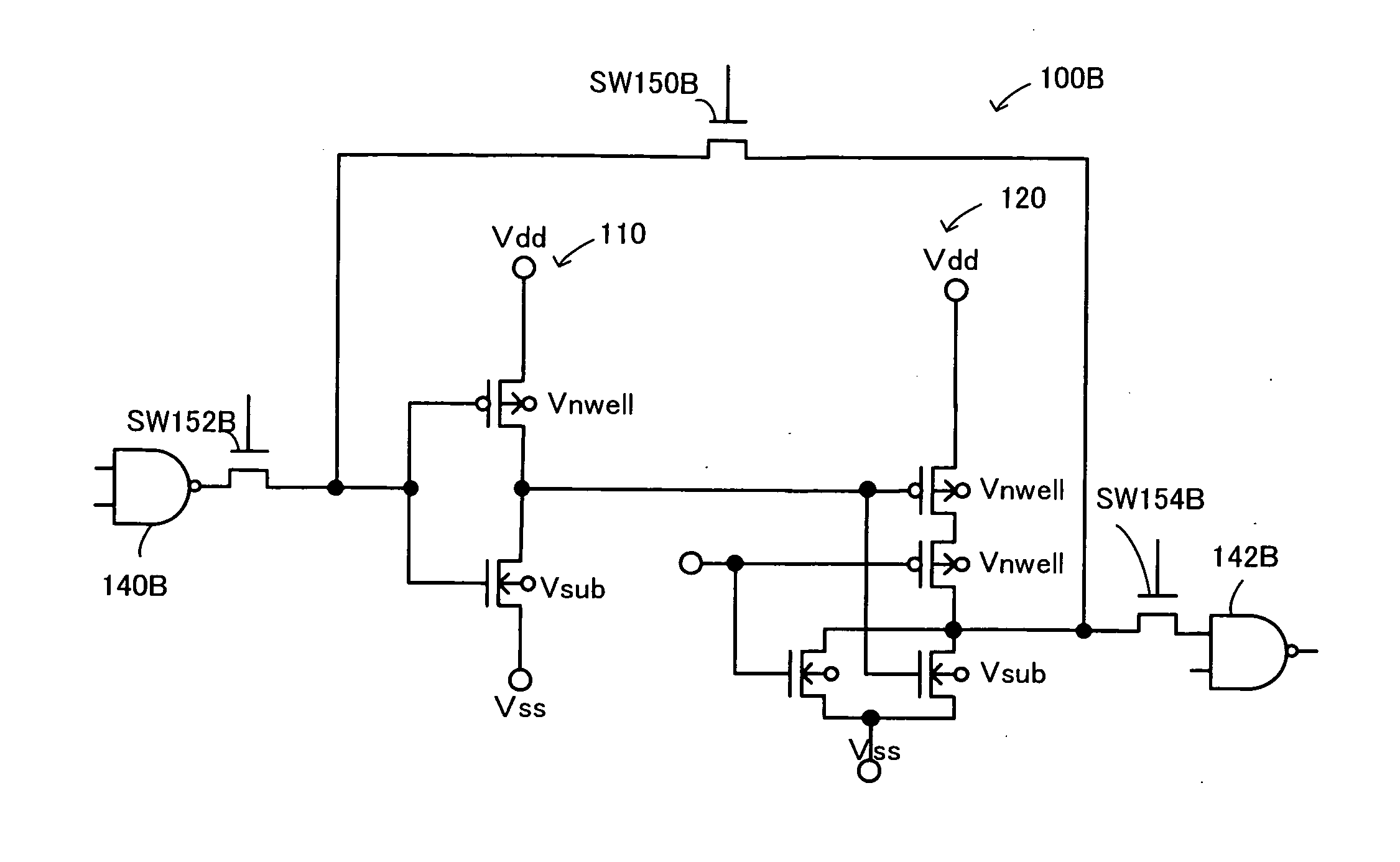
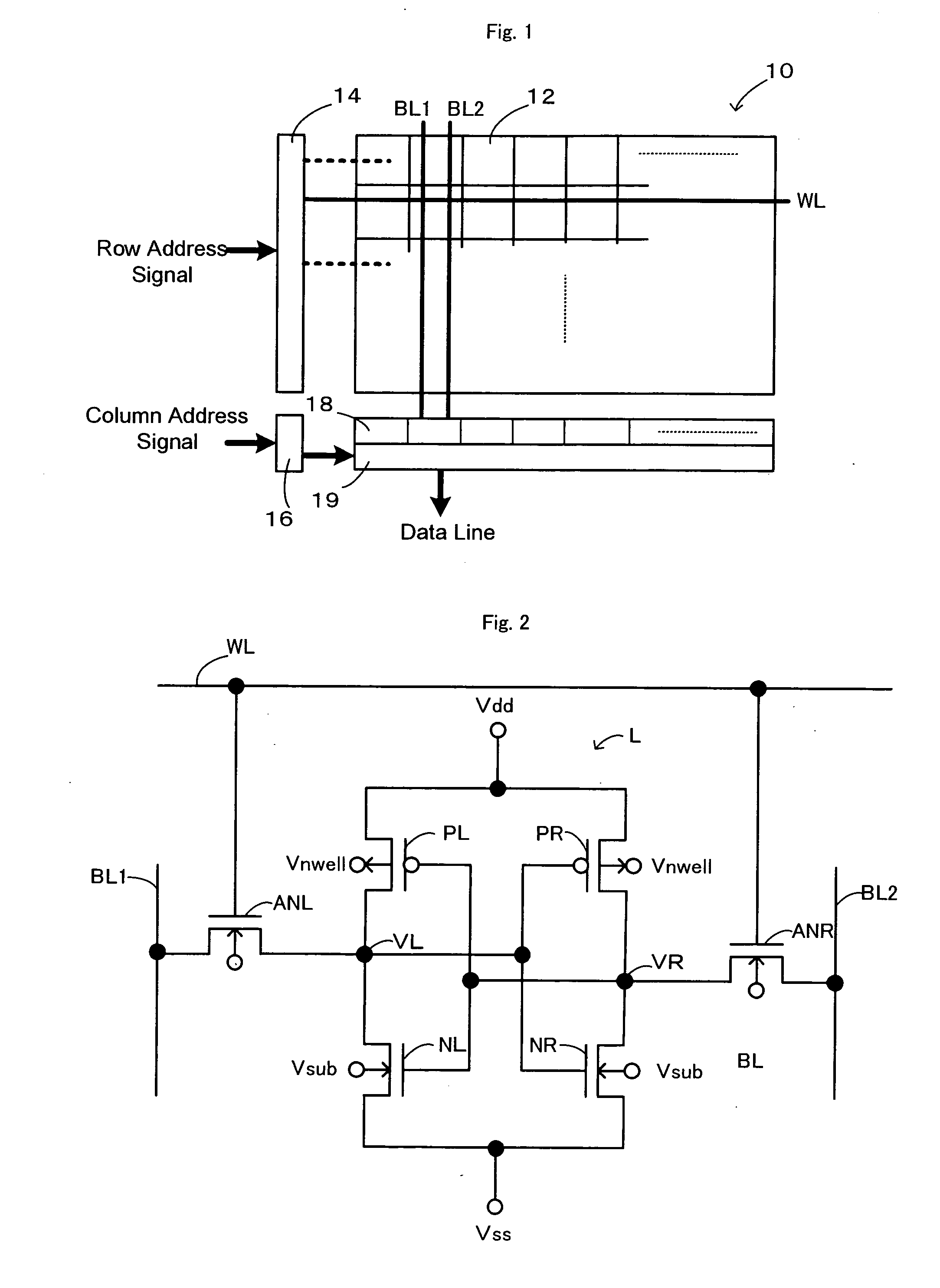
[0081]In the voltage characteristic regulating process of the second embodiment, voltages is applied to each of the power-supply voltage applied node Vdd, the ground voltage applied node Vss, the semiconductor substrate 20 and the well 30 of all memory cells of the SRAM 10 so that value of voltage Vdd becomes value of V2, the ground voltage Vss and the substrate voltage Vsub become 0V, and value of the well voltage Vnwell becomes value of V2. That is, the same voltage as voltage in the data readout operation (the same voltage as voltage Vdd, that is, value of V2) is applied to the all word lines WL and all bit lines BL1 and BL2 (step S100B). FIG. 14 schematically illustrates the butterfly curve in applying the voltage Vdd to the word line WL and the bit lines BL1 and BL2. Two largest squares that are inscribed in two curves obtained above are drawn. Static noise margin SNM is set to length of shorter diagonal line of diagonal line L1 and L2 of the two squares (in FIG. 14, length of ...

third embodiment

[0096]In the voltage characteristic regulating method of the third embodiment, the voltage is applied to each of the power-supply voltage applied node Vdd, the ground voltage applied node Vss, the semiconductor substrate 20, the well 30, the word line WL and the bit lines BL1 and BL2 of all memory cells of the RAM 310 so that voltage Vdd becomes value of V2, the ground voltage Vss and the substrate voltage Vsub become 0V, the well voltage Vnwell becomes value of V2, the word line voltage Vnwell becomes 0V, and the bit lines VBL1 and VBL2 become value of V2 (step S300). The state of each of the transistors of the memory cell 312 after executing the process of the step S300 reflects variation of current of the transistors PL, PR, NL and NR (current driving force). For illustrative purposes, each of current of the transistors PL and NR is set to be higher than that of the transistor PR or NL, the transistors PL and NR is turned on after executing of the process of the step S300, the no...


PUM


Abstract

The voltage Vdd is set to be lower than in the normal operation (step S100), then voltage is applied to each of the power-supply voltage applied node Vdd, the ground voltage applied node Vss, the semiconductor substrate and the well so that relative high voltage between the gate of turn-on transistor and the semiconductor substrate or the gate of turn-on transistor and well (steps S110 and S120). This process accomplishes rising of the threshold voltage of the transistor that is turned on, the reduction of the variation in the threshold voltage between a plurality of the transistors of the memory cell including latch circuit, and the improvement of the voltage characteristic of the memory cell.

Description

TECHNICAL FIELD[0001]The present invention relates to a voltage characteristic regulating method of latch circuit, a voltage characteristic regulating method of semiconductor device, and a voltage characteristic regulator of latch circuit, for details, a voltage characteristic regulating method, a voltage characteristic regulating method and a voltage characteristic regulator of latch circuit regulating voltage characteristic of the latch circuit comprising a plurality of gate type transistors that are formed in a semiconductor substrate.BACKGROUND ART[0002]A proposed method for regulating threshold voltage of gate type transistor, or MOS (Metal-Oxide-Semiconductor) transistor of a flash memory cell, that has a floating gate formed on a semiconductor substrate via a gate insulator film and a control gate formed on the floating gate via gate intervening insulator film includes adjusting threshold voltage of the MOS transistor by varying amount of electron accumulated in the floating ...

Claims


Application Information

Patent Timeline
Patent Type & Authority Applications(United States)
IPC IPC(8): G05F1/10
CPCG11C11/413
Inventor HIRAMOTO, TOSHIROSAKURAI, TAKAYASUSUZUKI, MAKOTO
Owner SEMICON TECH ACADEMIC RES CENT
Why Eureka
Try Eureka