
Liquid Chemical for Forming Protecting Film

a technology of liquid chemical and protective film, which is applied in the field of cleaning a, can solve the problems of inability to form water and pattern collapse cannot be prevented, and achieve the effects of preventing pattern collapse, excellent water repellency, and reducing throughpu

Active Publication Date: 2012-07-12
CENT GLASS CO LTD
View PDF5 Cites 11 Cited by
  • Summary
  • Abstract
  • Description
  • Claims
  • Application Information

AI Technical Summary

Benefits of technology

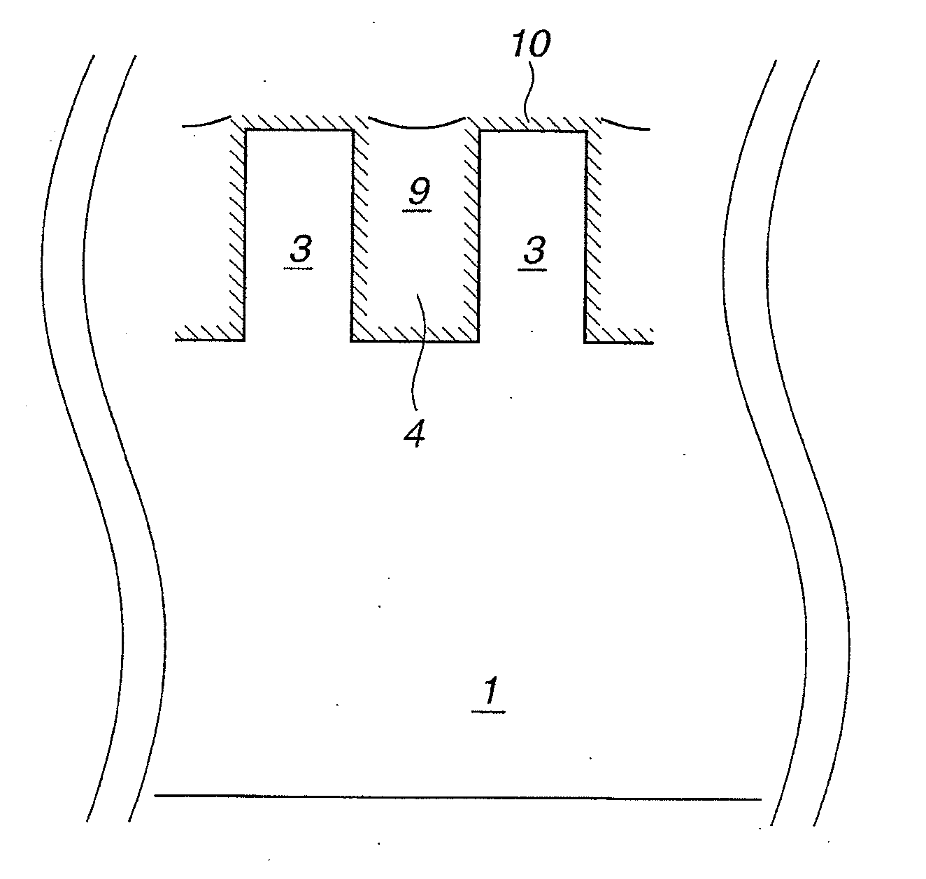
[0039]The protecting film formed from the liquid chemical for forming a protecting film, according to the present invention is excellent in water repellency. Therefore, in a wafer having at its surface an uneven pattern and containing at least one kind element of titanium, tungsten, aluminum, copper, tin, tantalum and ruthenium at surfaces of recessed portions of the uneven pattern, the film reduces the interaction between liquid retained in the recessed portions and the surfaces of the recessed portions, and by extension brings about the effect of preventing the pattern collapse. By using the liquid chemical, a cleaning step conducted in a method for producing the wafer having at its surface an uneven pattern is improved without lowering throughput. Accordingly, the method for producing the wafer having the uneven pattern at its surface, conducted in the use of the liquid chemical for forming a protecting film of the present invention, is excellent in productivity.
[0040]The liquid chemical for forming a protecting film, according to the present invention is adaptable to uneven patterns having the aspect ratio expected to rise more and more, for example, an aspect ratio of not less than 7, which allows cost reduction in producing more sophisticated semiconductor devices. In addition, the liquid chemical is adaptable without considerably modifying conventional apparatuses and therefore results in being one applicable in production of various kinds of semiconductor devices.

Problems solved by technology

However, in a case where a wafer having at its surface a substance that does not sufficiently contain reactive functional groups (e.g., silanol groups), such as the wafer containing the above-mentioned metal-based element at its surface, it is not possible to form a water-repellent protecting film for preventing the pattern collapse even if the treatment liquid or treatment method discussed in Patent Publications 3 to 5 is used, which is a problem in that the pattern collapse cannot be prevented.

Method used


Image

  • Liquid Chemical for Forming Protecting Film
  • Liquid Chemical for Forming Protecting Film
  • Liquid Chemical for Forming Protecting Film

Examples


example 1

(I-1) Preparation of Liquid Chemical for Forming Protecting Film

[0129]A mixture of 0.002 g of octadecylphosphonic acid [C18H37P(O)(OH)2] serving as an agent for forming a water-repellent protecting film and 99.998 g of propylene glycol monomethyl ether acetate (hereinafter referred to as “PGMEA”) serving as an organic solvent was stirred for about 18 hours thereby obtaining a liquid chemical for forming a protecting film, in which liquid chemical the protecting-film-forming agent had a concentration of 20 mass ppm relative to the total quantity of the liquid chemical for forming a protecting film (hereinafter referred to as “a protecting-film-forming agent concentration”).

(I-2) Step of Cleaning Wafer (Pretreatment Step)

[0130]As a pretreatment step 2, a wafer having a smooth titanium nitride film (a silicon wafer formed having on its surface a titanium nitride layer of 50 nm thickness) was immersed in 1 mass % aqueous hydrogen peroxide for 1 minute at room temperature, and then immer...

examples 2 to 84

[0133]Upon suitably modifying those used in Example 1 (i.e., the protecting-film-forming agent, the solvent for the liquid chemical for forming a protecting film, the protecting-film-forming agent concentration, the time for the protecting-film-forming step, the temperature of the protecting-film-forming step and the cleaning liquid for the subsequent cleaning step), the surface treatment was conducted on a wafer. Then, evaluations were performed thereon. The results are shown in Table 1 to Table 3.

TABLE 2Liquid chemical for forming protecting filmProtecting-film-Protecting-film-Cleaningforming stepforming agentliquid forTempera-Protecting-film-concentrationpretreatmenttureTimeforming agentSolvent[mass ppm]Waferstep 3[C. °][min]Example 31C6F13—C2H4—P(O) (OH)2Cyclohexanone100TiNiPA2010Example 32C6F13—C2H4—P(O) (OH)2iPA100TiNiPA2010Example 33C6F13—C2H4—P(O) (OH)2Water100TiNiPA2010Example 34C6F13—C2H4—P(O) (OH)2Water100TiNiPA4010Example 35C6F13—C2H4—P(O) (OH)2PGME100TiNiPA2010Example 3...

example 85

(II-1) Preparation of Liquid Chemical for Forming Protecting Film

[0135]A mixture of 0.002 g of octadecylphosphonic acid [C18H37P(O)(OH)2] serving as an agent for forming a water-repellent protecting film and 99.998 g of PGMEA serving as an organic solvent was stirred for about 18 hours thereby obtaining a liquid chemical for forming a protecting film, in which liquid chemical the protecting-film-forming agent concentration was 20 mass ppm.

(II-2) Step of Cleaning Wafer (Pretreatment Step)

[0136]As a pretreatment step 2, a wafer having a smooth tungsten film (a silicon wafer formed having on its surface a tungsten layer of 50 nm thickness) was immersed in 1 mass % aqueous ammonia for 1 minute at room temperature, and then immersed in pure water for 1 minute. Furthermore, as a pretreatment step 3, the wafer was immersed in iPA for 1 minute.

(II-3) From Step of Forming Protecting Film on Wafer Surface to Drying Step

[0137]As a protecting-film-forming step, the wafer having the tungsten fil...


PUM

PropertyMeasurementUnit
aspect ratioaaaaaaaaaa
power consumptionaaaaaaaaaa
aspect ratioaaaaaaaaaa

Abstract

Disclosed is a liquid chemical for forming a water-repellent protecting film. The liquid chemical contains an agent for forming a water-repellent protecting film, and a solvent. The agent is for provided to form a water-repellent protecting film on a wafer after a cleaning step for the wafer and before a drying step for the wafer, the wafer having at its surface an uneven pattern and containing at least one kind element of titanium, tungsten, aluminum, copper, tin, tantalum and ruthenium at surfaces of recessed portions of the uneven pattern, the water-repellent protecting film being formed at least on the surfaces of the recessed portions. The liquid chemical is characterized in that the agent for forming a water-repellent protecting film is a compound represented by the following general formula [1].

Description

BACKGROUND OF THE INVENTION[0001]The present invention relates to a technique of cleaning a substrate (a wafer) in semiconductor device fabrication or the like.[0002]Semiconductor devices for use in networks or digital household electric appliances are desired to be further sophisticated and multifunctional, and to be low in power consumption. Accordingly, the trend toward micro-patterning for circuits is continuing. Together with the continuation of micro-patterning, a pattern collapse in the circuits has become a significant problem. In semiconductor device fabrication, a cleaning step is greatly used for the purpose of removing particles and metal impurities. As a result of this, the cleaning step occupies 30-40% of the whole of the semiconductor fabrication step. A phenomenon observed in the cleaning step when an aspect ratio of pattern is high due to the micro-patterning for semiconductor device is a pattern collapse, in which a gas-liquid interface that comes about collapses t...

Claims


Application Information

Patent Timeline
Patent Type & Authority Applications(United States)
IPC IPC(8): B08B3/10C09D5/00
CPCH01L21/02068H01L21/302C09K3/18C11D2111/22
Inventor SAIO, TAKASHIKUMON, SOICHISAITO, MASANORIARATA, SHINOBUNANAI, HIDEHISAAKAMATSU, YOSHINORI
Owner CENT GLASS CO LTD
Learn More