
Integrated circuit, method for driving the same, and semiconductor device

a technology of integrated circuits and semiconductor devices, applied in the field of integrated circuits, can solve the problems of shortening the travel distance per certain amount of charge, affecting the operation speed of semiconductor circuits, and reducing the power consumption of semiconductor circuits, so as to achieve the effect of reducing the operation speed and reducing the power consumption

Active Publication Date: 2012-06-07
SEMICON ENERGY LAB CO LTD
View PDF6 Cites 40 Cited by
  • Summary
  • Abstract
  • Description
  • Claims
  • Application Information

AI Technical Summary

Benefits of technology

[0016]Thus, the inventors perform data retention in each FF included in an integrated circuit. The FF is a sequential logic circuit for retaining 1-bit data. Consequently, when data is retained in each FF, even in the case of a huge integrated circuit or the like including countless FFs, each of a plurality of FFs may transfer data per bit, data in the countless FFs can be transferred only in a transfer time of 1-bit data, and the integrated circuit can be switched to a resting state rapidly.
[0038]According to the present invention, it is possible to provide an integrated circuit which can be switched to a resting state and can be returned from the resting state rapidly. It is possible to provide an integrated circuit whose power consumption can be reduced without the decrease in operation speed. It is possible to provide a method for driving the integrated circuit.

Problems solved by technology

In particular, in a portable electronic device, power is supplied from a battery, and the uptime is limited due to a limited amount of power.
For example, in the case of an electric car, leakage current of an in-car electronic device shortens the travel distance per certain amount of charge.
Note that in the case where the semiconductor circuit included in the integrated circuit is volatile, when the power of the integrated circuit is turned off, data which is being processed in the semiconductor circuit is lost.
However, in the case of a huge integrated circuit or the like including countless FFs, it is necessary to write a large amount of data retained in the countless FFs to a memory circuit portion.
Thus, in the case where the memory circuit portion is provided separately from the integrated circuit, a large amount of data is transferred through a limited number of signal lines.
Consequently, it takes time to write data from the integrated circuit to the memory circuit portion, so that it is impossible to switch the integrated circuit to a resting state rapidly.
Thus, it is difficult to return the integrated circuit from the resting state at high speed.

Method used


Image

  • Integrated circuit, method for driving the same, and semiconductor device
  • Integrated circuit, method for driving the same, and semiconductor device
  • Integrated circuit, method for driving the same, and semiconductor device

Examples


embodiment 1

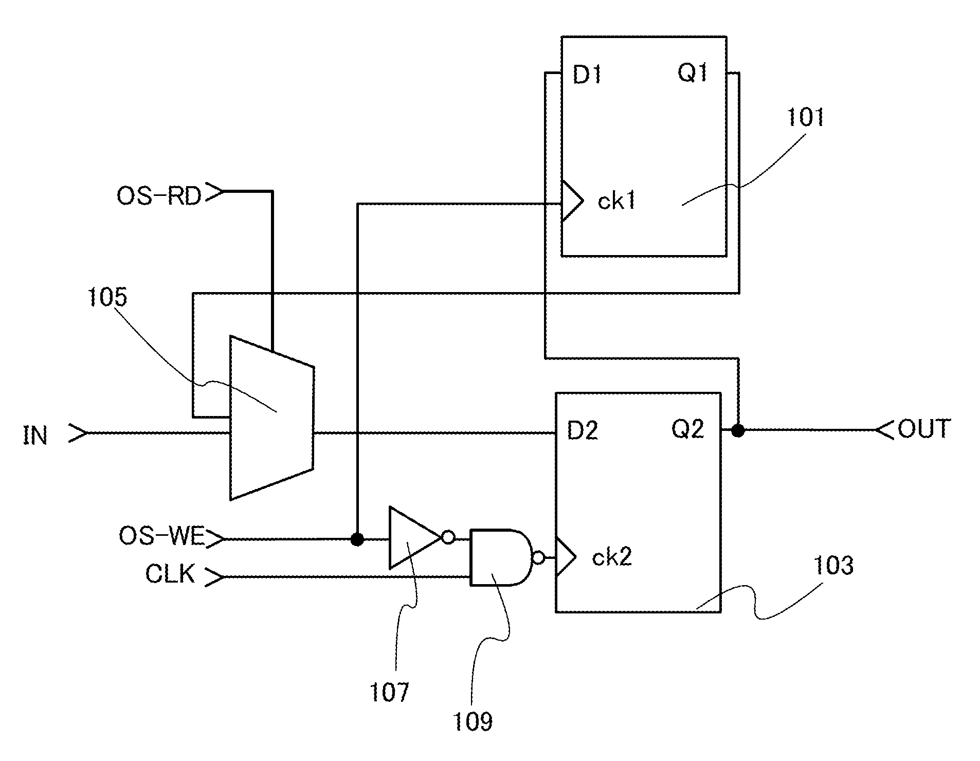
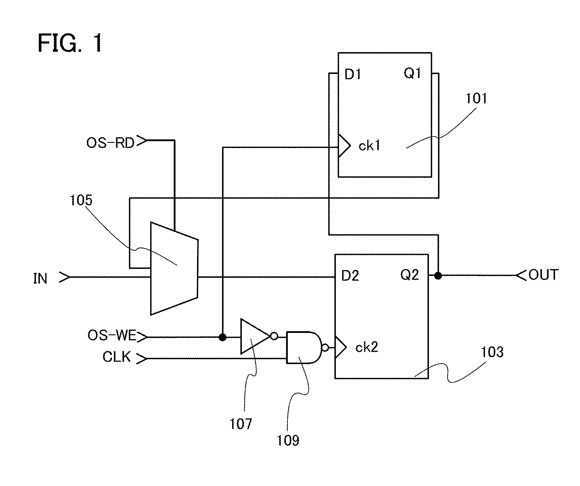
[0051]In this embodiment, a semiconductor circuit used for an integrated circuit in one embodiment of the present invention is described. The integrated circuit in one embodiment of the present invention includes a plurality of semiconductor circuits described in this embodiment. FIG. 1 illustrates the semiconductor circuit in this embodiment.

[0052]The semiconductor circuit illustrated in FIG. 1 includes a nonvolatile FF 101, a volatile FF 103, a selection circuit 105, an inverter circuit 107, and a NAND circuit 109. A first control signal (OS-RD), a second control signal (OS-WE), a clock signal (CLK), external input data (N) are input to the semiconductor circuit, and external output data (OUT) is output from the semiconductor circuit.

[0053]The nonvolatile FF 101 includes an input terminal (D1), an output terminal (Q1), and a clock input terminal (ck1). The output terminal (Q1) of the nonvolatile FF 101 is electrically connected to one input terminal of the selection circuit 105. T...

embodiment 2

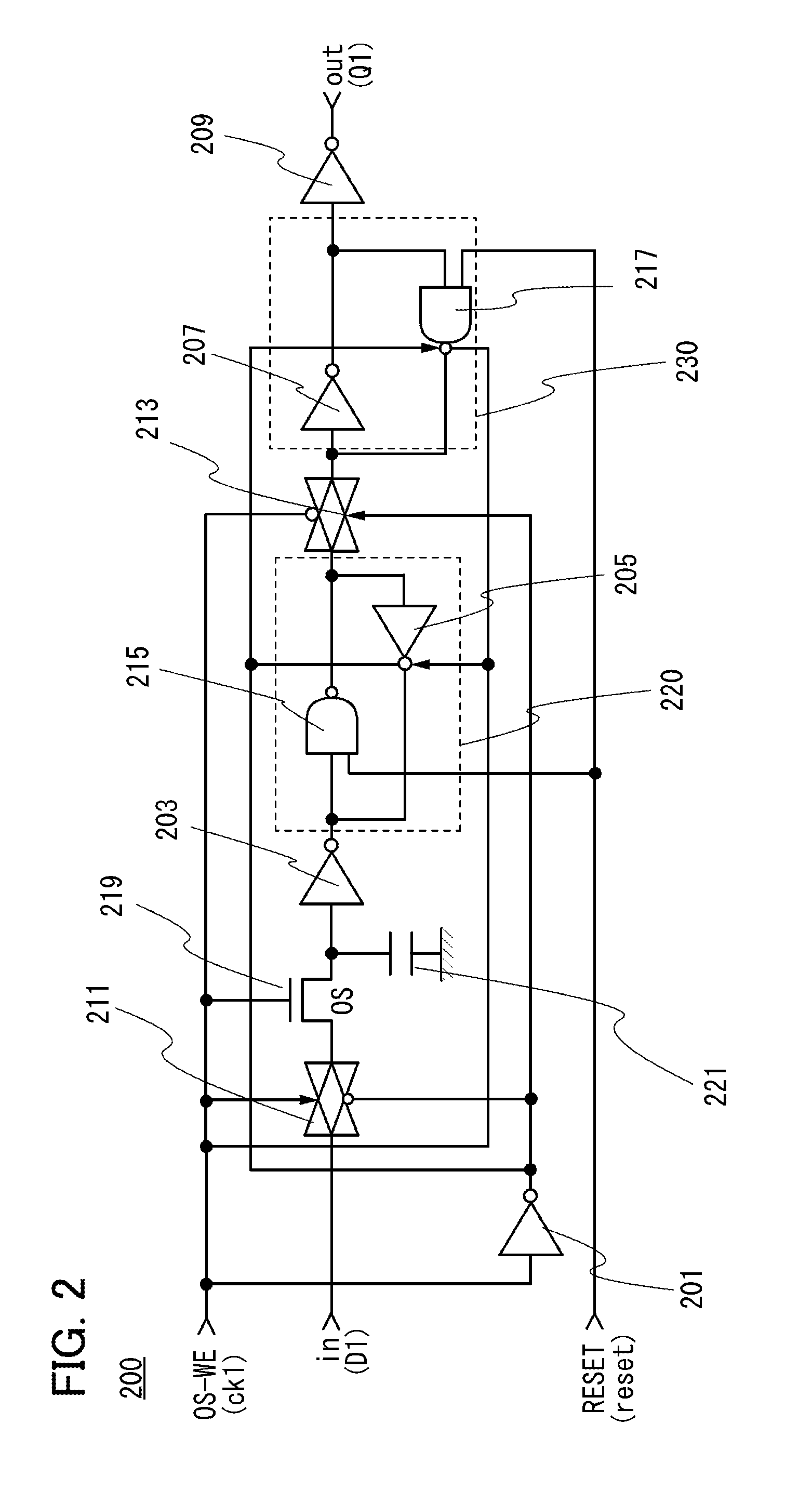
[0103]In this embodiment, the circuit structure of the nonvolatile FF in Embodiment 1 is described. FIG. 2 illustrates an example of the circuit structure of the nonvolatile FF.

[0104]The nonvolatile FF includes a memory circuit and an arithmetic portion. A nonvolatile FF 200 illustrated in FIG. 2 includes a transistor 219 including an oxide semiconductor in a semiconductor layer and a storage capacitor 221 as the memory circuit, and a first inverter circuit 203, a second inverter circuit 209, a first analog switch 211, a second analog switch 213, a first latch circuit 220, and a second latch circuit 230 as the arithmetic portion.

[0105]The transistor 219 has a gate electrode, a first electrode, and a second electrode, and includes an oxide semiconductor in the semiconductor layer. A channel formation region of the transistor 219 includes a highly purified oxide semiconductor; thus, the transistor 219 has extremely low off-state current.

[0106]The gate electrode of the transistor 219 i...

embodiment 3

[0147]In this embodiment, a structure and a manufacturing method of an integrated circuit in one embodiment of the present invention are described with reference to FIGS. 5A to 5C, FIGS. 6A to 6D, FIGS. 7A to 7D, FIGS. 8A to 8D, and FIGS. 9A to 9C.

[0148]FIG. 5C illustrates the circuit structure of a semiconductor circuit in this embodiment. The semiconductor circuit in this embodiment includes a transistor 562 including an oxide semiconductor in a semiconductor layer, a transistor 560 including a material other than an oxide semiconductor in a semiconductor layer, and a storage capacitor 564. The semiconductor circuit in this embodiment is part of the integrated circuit or part of the semiconductor circuit described in Embodiments 1 and 2. For example, the transistor 562, the storage capacitor 564, and the transistor 560 can be used as the transistor 219 included in the nonvolatile FF 200, the storage capacitor 221, and the transistor included in the first inverter circuit 203 in FI...


PUM


Abstract

An integrated circuit which can be switched to a resting state and can be returned from the resting state rapidly is provided. An integrated circuit whose power consumption can be reduced without the decrease in operation speed is provided. A method for driving the integrated circuit is provided. The integrated circuit includes a first flip-flop and a second flip-flop including a nonvolatile memory circuit. In an operating state in which power is supplied, the first flip-flop retains data. In a resting state in which supply of power is stopped, the second flip-flop retains data. On transition from the operating state into the resting state, the data is transferred from the first flip-flop to the second flip-flop. On return from the resting state to the operating state, the data is transferred from the second flip-flop to the first flip-flop.

Description

BACKGROUND OF THE INVENTION[0001]1. Field of the Invention[0002]The present invention relates to a semiconductor circuit, an integrated circuit including a plurality of semiconductor circuits, a method for driving the integrated circuit, and a semiconductor device including the integrated circuit.[0003]2. Description of the Related Art[0004]In recent years, the information society has been increasingly developed, and the demand for higher speed, higher capacity, smaller size, lighter weight, or the like of a personal computer, a cellular phone, or the like has been increased. In the tide of the times, a large-scale integrated circuit (large scale integration (LSI)) and a central processing unit (CPU) need higher integration, higher operation speed, and lower power consumption.[0005]An integrated circuit such as an LSI or a CPU is mounted on a circuit board or a printed wiring board and is used as one of the components of a variety of electronic devices.[0006]An electronic device inc...

Claims


Application Information

Patent Timeline
IPC IPC(8): G11C11/24G11C11/00
CPCH03K3/356008H03K3/012H03K21/403H03K21/023
Inventor ENDO, MASAMIOHMARU, TAKURO
Owner SEMICON ENERGY LAB CO LTD
Learn More