Optical sensor and display apparatus
- Summary
- Abstract
- Description
- Claims
- Application Information
AI Technical Summary
Benefits of technology
Problems solved by technology
Method used
Image

Examples
first embodiment
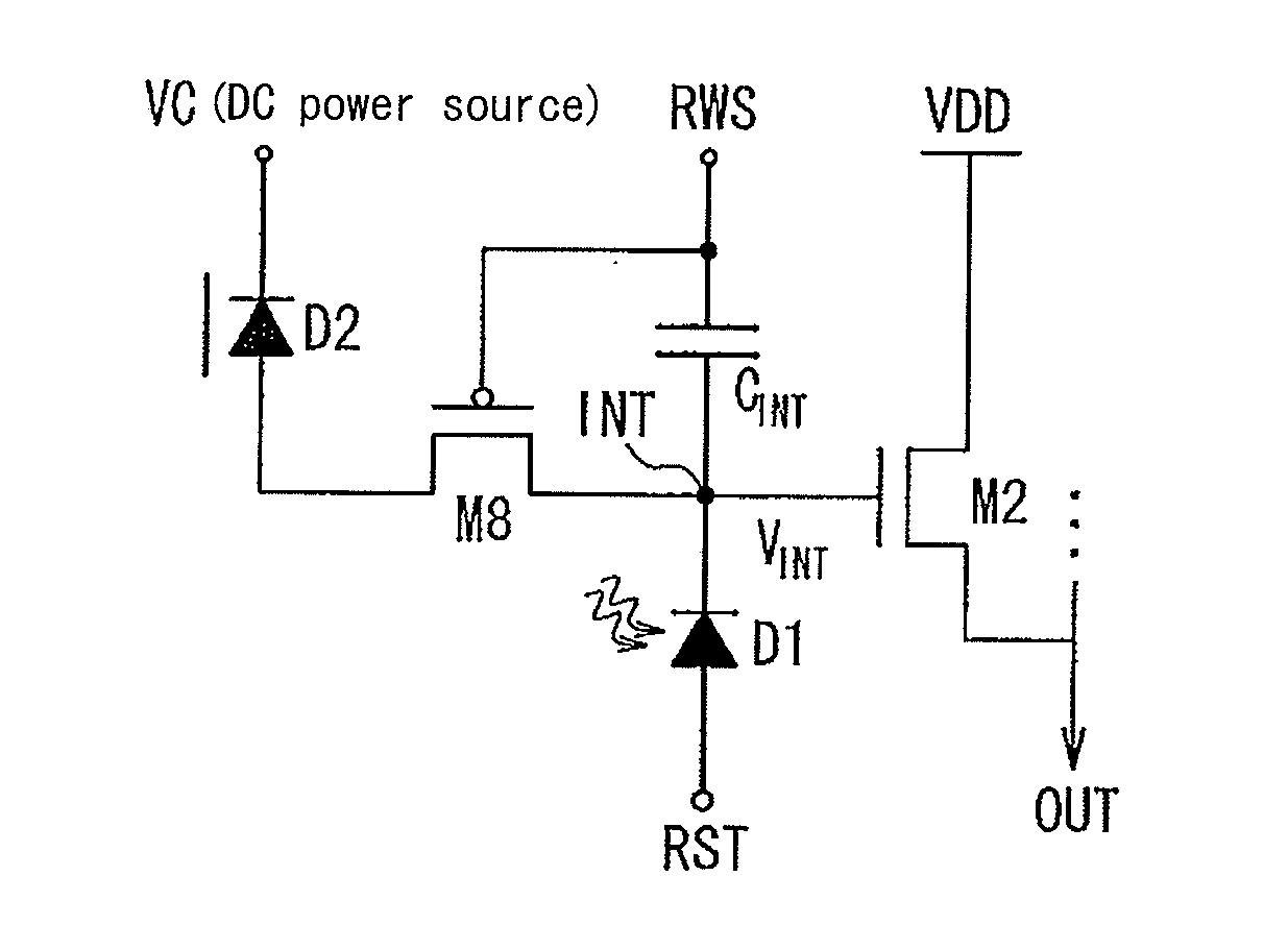
[0058]FIG. 1 shows a circuit configuration of an optical sensor according to An optical sensor shown in FIG. 1 includes photodiodes D1 and D2, a capacitor CINT (accumulation capacitor), a thin-film transistor M2 (first switching element), and a p-channel thin-film transistor M8 (second switching element). The photodiode D1 is an exemplary photodetecting element through which an electric current flows according to an amount of received incident light, and the photodiode D2 is an exemplary reference element having a light-shielding layer for shielding incident light.
[0059]The photodiodes D1 and D2 have circuit characteristics or element characteristics that are optimized so that output electric currents when no light is projected thereto are equal. Since I-V characteristics (reverse-bias region) of photodiodes do not depend on an applied voltage, ideally, dark currents of the photodiodes D1 and D2 are equal to each other in the case where the sizes (a length L and a width W of a semi...
second embodiment
[0082]First, a configuration of a liquid crystal display device that includes an optical sensor of the present invention is explained, with reference to FIGS. 5 and 6.
[0083]FIG. 5 is a block diagram showing a schematic configuration of an active matrix substrate 100 provided in a liquid crystal display device according to one embodiment of the present invention. As shown in FIG. 5, the active matrix substrate 100 includes, on its glass substrate, at least a pixel region 1, a display gate driver 2, a display source driver 3, a sensor column driver 4, a sensor row driver 5, a buffer amplifier 6, and an FPC connector 7. Further, a signal processing circuit 8 for processing an image signal captured by a photodetecting element (to be described later) in the pixel region 1 is connected with the active matrix substrate 100 via the FPC connector 7 and a FPC 9.
[0084]It should be noted that the above-described members on the active matrix substrate 100 may be formed monolithically on the gla...
third embodiment
[0122]FIG. 14 is a timing chart showing waveforms of a reset signal supplied from a line RST to the optical sensor and a readout signal supplied from a line RWS to the optical sensor. FIG. 15 is a waveform diagram showing a relationship between input signals (RST, RWS) and VINT in the optical sensor according to
[0123]The high level VRST.H of the reset signal is set to a potential that causes the thin-film transistor M2 to be turned on. In the example shown in FIG. 14, the high level VRST.H of the reset signal is 8 V. The reset signal has a low level VRST.L of 0 V. In this example, the high level VRST.H of the reset signal is equal to VDD, and the low level VRST.L thereof is equal to VSS. Further, the high level VRWS.H of the readout signal is 8 V, and the low level VRWS.L thereof is 0 V. In this example, the high level VRWS.H of the readout signal is equal to VDD, and the low level VRWS.L thereof is equal to VSS.
[0124]First, when the reset signal supplied from the sensor row driver ...
PUM
 Abstract
Description
Claims
Application Information
 - R&D
- Intellectual Property
- Life Sciences
- Materials
- Tech Scout
- Unparalleled Data Quality
- Higher Quality Content
- 60% Fewer Hallucinations
Browse by: Latest US Patents, China's latest patents, Technical Efficacy Thesaurus, Application Domain, Technology Topic, Popular Technical Reports.
© 2025 PatSnap. All rights reserved.Legal|Privacy policy|Modern Slavery Act Transparency Statement|Sitemap|About US| Contact US: help@patsnap.com