Semiconductor wafer, method of producing semiconductor wafer, and electronic device

a semiconductor wafer and semiconductor technology, applied in the direction of semiconductor devices, electrical devices, transistors, etc., can solve the problems of leakage current, insufficient device isolation, and difficulty in optimizing the characteristics of both devices formed on the single semiconductor wafer

Inactive Publication Date: 2012-02-02
SUMITOMO CHEM CO LTD
View PDF17 Cites 12 Cited by
  • Summary
  • Abstract
  • Description
  • Claims
  • Application Information

AI Technical Summary

Benefits of technology

[0020]According to the third aspect related to the present invention, provided is one exemplary electronic device including a first semiconductor, a carrier-trapping layer formed on the first semiconductor, a second semiconductor that is epitaxially grown on the carrier-trapping layer and serves as a channel in which a free electron or a free hole moves, a third semiconductor including a stack represented by n-type semiconductor / p-type semiconductor / n-type semiconductor or represented by p-type semiconductor / n-type semiconductor / p-type semiconductor, where the stack epitaxially grown on the second semiconductor, a field-effect transistor formed in the second semiconductor, and a heterojunction bipolar transistor formed in the third semiconductor.
[0021]As used herein, “B on A” refers to both of the case where “B is in contact with A” and the case where “there are one or more intervening elements between A and B.”

Problems solved by technology

The residual impurities generate carriers between the FET and the semiconductor wafer and cause leakage currents.
The generated carriers may result in the insufficient device isolation.
Furthermore, it may be difficult to optimize the characteristics of both of the devices formed on the single semiconductor wafer.

Method used


Image

  • Semiconductor wafer, method of producing semiconductor wafer, and electronic device
  • Semiconductor wafer, method of producing semiconductor wafer, and electronic device
  • Semiconductor wafer, method of producing semiconductor wafer, and electronic device

Examples


example experiment 1

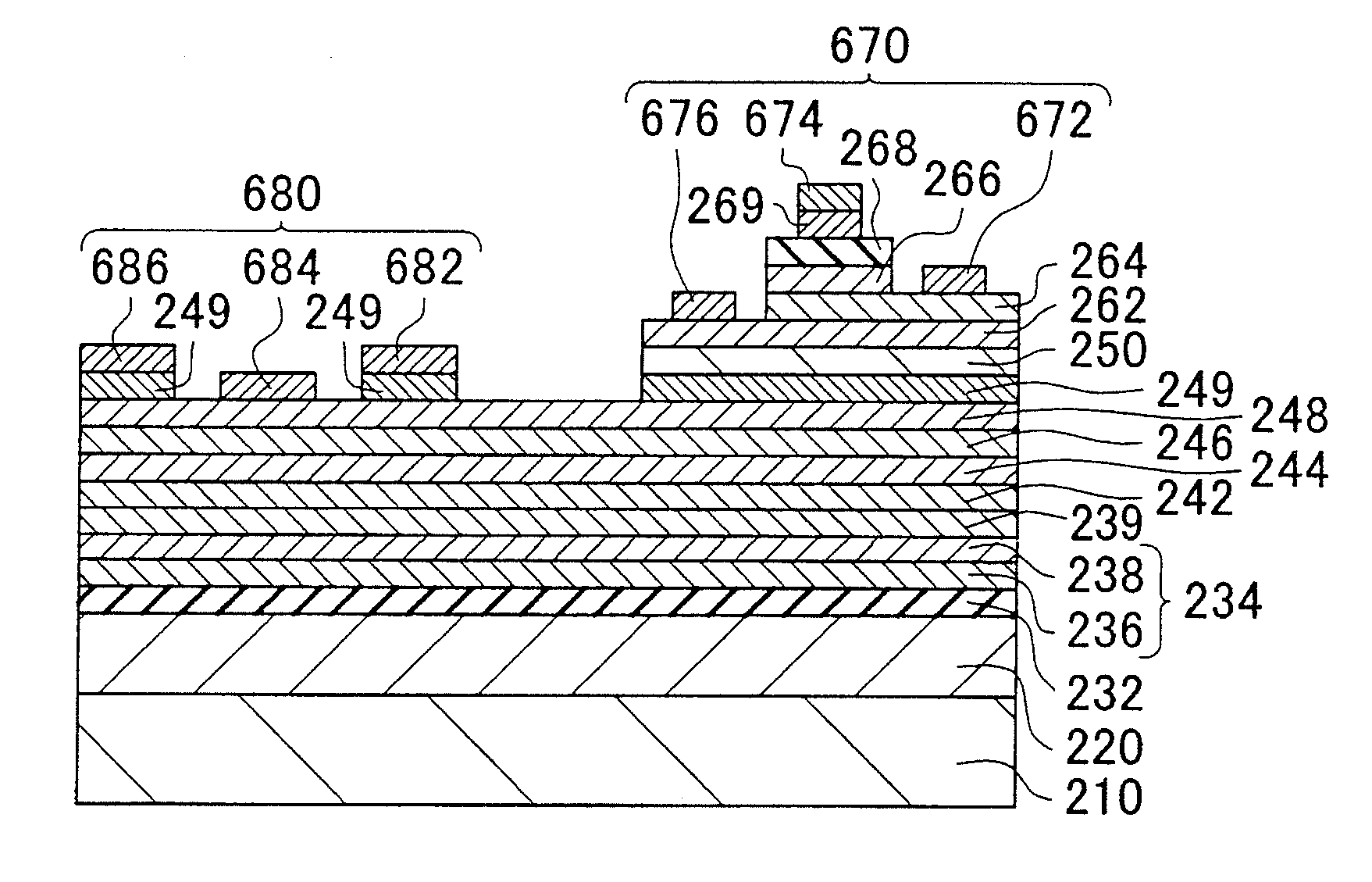
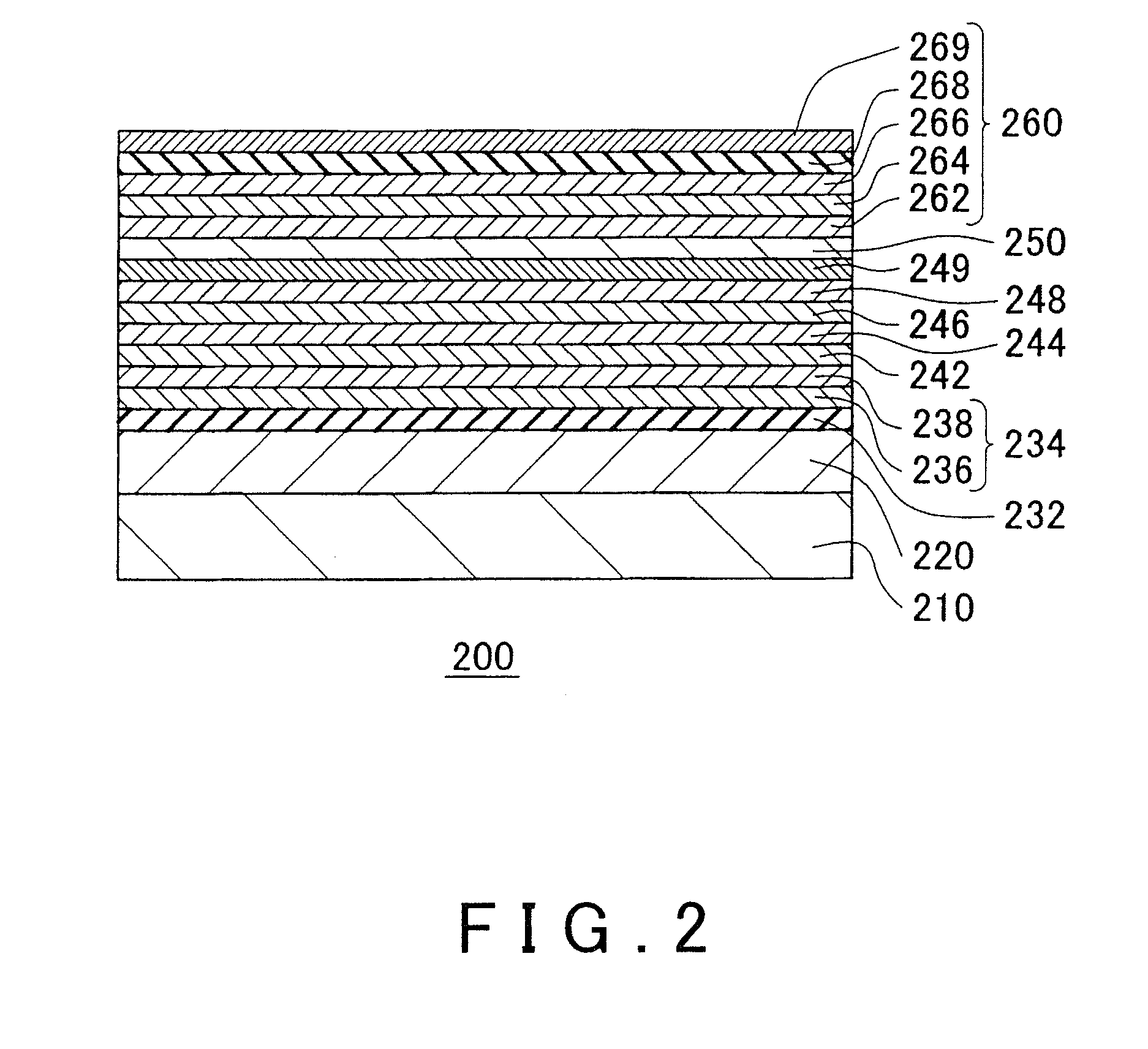
[0098]In Example Experiment 1, a semiconductor wafer was fabricated that includes all the semiconductor layers of the semiconductor wafer 200 shown in FIG. 2 except for the semiconductor layers from the contact layer 249 to the contact layer 269. A GaAs single-crystal wafer was used as the first semiconductor 210. An i-type GaAs was formed as the buffer layer 220 and oxygen-doped i-type AlGaAs was formed as the carrier-trapping layer 232.

[0099]As the depleted semiconductor 234, a lightly-doped p-type semiconductor layer was formed that has five sets of alternately stacked GaAs and AlGaAs while the molar supply ratio of the Group 5 source to the Group 3 source was regulated. As the carrier-supplying semiconductor 242 and the carrier-supplying semiconductor 246, n-type AlGaAs was formed. As the carrier movement layer 244, i-type InGaAs was formed. As the barrier-forming semiconductor 248, i-type AlGaAs was formed.

[0100]The respective semiconductor layers from the buffer semiconductor ...

example experiment 2

[0101]In Example Experiment 2, a semiconductor wafer was fabricated that is the same as the semiconductor wafer of Example Experiment 1 except for that the semiconductor layer corresponding to the depleted semiconductor 234 was a low-concentration impurity layer with n carrier type. In Example Experiment 2, since the semiconductor layer corresponding to the depleted semiconductor 234 is a low-concentration n-type layer, the fabricated semiconductor wafer had no depleted region.

[0102]The withstand voltages of the semiconductor wafers fabricated in Example Experiment 1 and Example Experiment 2 were measured and respectively 34 V for Example Experiment 1 and 7 V for Example Experiment 2. This result proves that Example Experiment 1 achieves improved withstand voltage since the depleted semiconductor 234 forms a depleted region. Here, the withstand voltage is defined as a voltage that yields a current density of 5 mA / cm2 between the first semiconductor 210 and the carrier-supplying semi...

example experiment 3

(Example Experiment 3

[0103]A semiconductor wafer was fabricated that is the same as the semiconductor wafer of Example Experiment 1 except for that the thickness of the carrier-trapping layer 232 was varied among 20 nm, 100 nm, and 150 nm, the oxygen concentration of the carrier-trapping layer 232 was set at 7×1019 cm−3, and the thickness of the depleted semiconductor 234 was set at 300 nm. The withstand voltage of the fabricated semiconductor wafer is shown in FIG. 6 as a function of the thickness of the carrier-trapping layer 232. FIG. 6 reveals that the withstand voltage increases as the thickness of the carrier-trapping layer 232 increases. In particular, the withstand voltage was remarkably improved when the carrier-trapping layer 232 had a thickness of 100 nm or more.


PUM


Abstract

There is provided a compound semiconductor wafer that is suitably used as a semiconductor wafer to form a plurality of different types of devices such as an HBT and an FET thereon. The semiconductor wafer includes a first semiconductor, a carrier-trapping layer that is formed on the first semiconductor and has an electron-trapping center or a hole-trapping center, a second semiconductor that is epitaxially grown on the carrier-trapping layer and serves as a channel in which a free electron or a free hole moves, and a third semiconductor including a stack represented by n-type semiconductor/p-type semiconductor/n-type semiconductor or represented by p-type semiconductor/n-type semiconductor/p-type semiconductor, where the stack epitaxially grown on the second semiconductor.

Description

CROSS REFERENCE TO RELATED APPLICATION[0001]The contents of the following Japanese patent application and PCT patent application are incorporated herein by reference:[0002]JP 2009-093442 filed on Apr. 7, 2009, and[0003]PCT / JP2010 / 002449 filed on Apr. 2, 2010.BACKGROUND[0004]1. Technical Field[0005]The present invention relates to a semiconductor wafer, a method of producing a semiconductor wafer, and an electronic device.[0006]2. Related Art[0007]JP 2008-060554 A discloses a method of producing an epitaxial Group 3-5 compound semiconductor wafer that is suitable for fabricating at least two different types of integrated active devices (for example, an HBT and an FET) thereon.[0008]When a plurality of different types of devices, for example, a heterojunction bipolar transistor (HBT) and a field-effect transistor (FET), are formed on a single semiconductor wafer, the manufacturing process of one of the devices may affect the manufacturing process of the other device.[0009]For example,...

Claims


Application Information

Patent Timeline
Patent Type & Authority Applications(United States)
IPC IPC(8): H01L29/267H01L21/20
CPCH01L21/8252H01L27/0605H01L29/7786H01L29/7785H01L29/7371H01L21/326H01L21/8222H01L29/73
Inventor ICHIKAWA, OSAMU
Owner SUMITOMO CHEM CO LTD
Why Eureka
Try Eureka