Semiconductor process

a technology of semiconductor devices and process steps, applied in the direction of semiconductor devices, basic electric elements, electrical equipment, etc., can solve the problems of circuit leakage, low electrical quality of semiconductor devices, and the inability to increase the driving current of mos transistors, etc., and achieve the effect of good electrical quality

Active Publication Date: 2012-01-26
UNITED MICROELECTRONICS CORP
View PDF3 Cites 14 Cited by
  • Summary
  • Abstract
  • Description
  • Claims
  • Application Information

AI Technical Summary

Benefits of technology

[0009]It is another objective of the present invention to provide a semiconductor process of using an etchant including NH4OH / H2O2 for forming a semiconductor device having well electrical quality.

Problems solved by technology

As the semiconductor processes advance to very deep sub micron era such as 65-nm node or beyond, how to increase the driving current for MOS transistors has become a critical issue.
It is should be noted that a recess etched by ammonia water has a V-shaped profile and the V-shaped profile typically results in circuit leakages and diminishes the electrical quality of the semiconductor device.
Moreover, as the dimension of semiconductor devices scales down as the industry develops, the aforementioned issue of the recess profile affecting electrical property of the product also worsens substantially.

Method used


Image

  • Semiconductor process
  • Semiconductor process
  • Semiconductor process

Examples


Embodiment Construction

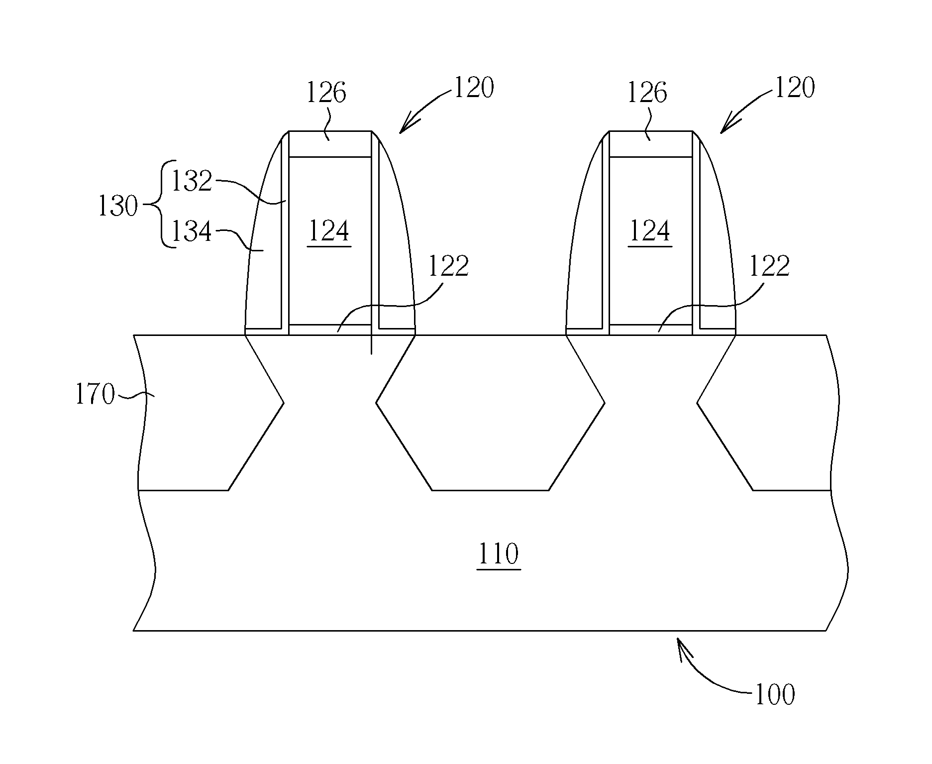
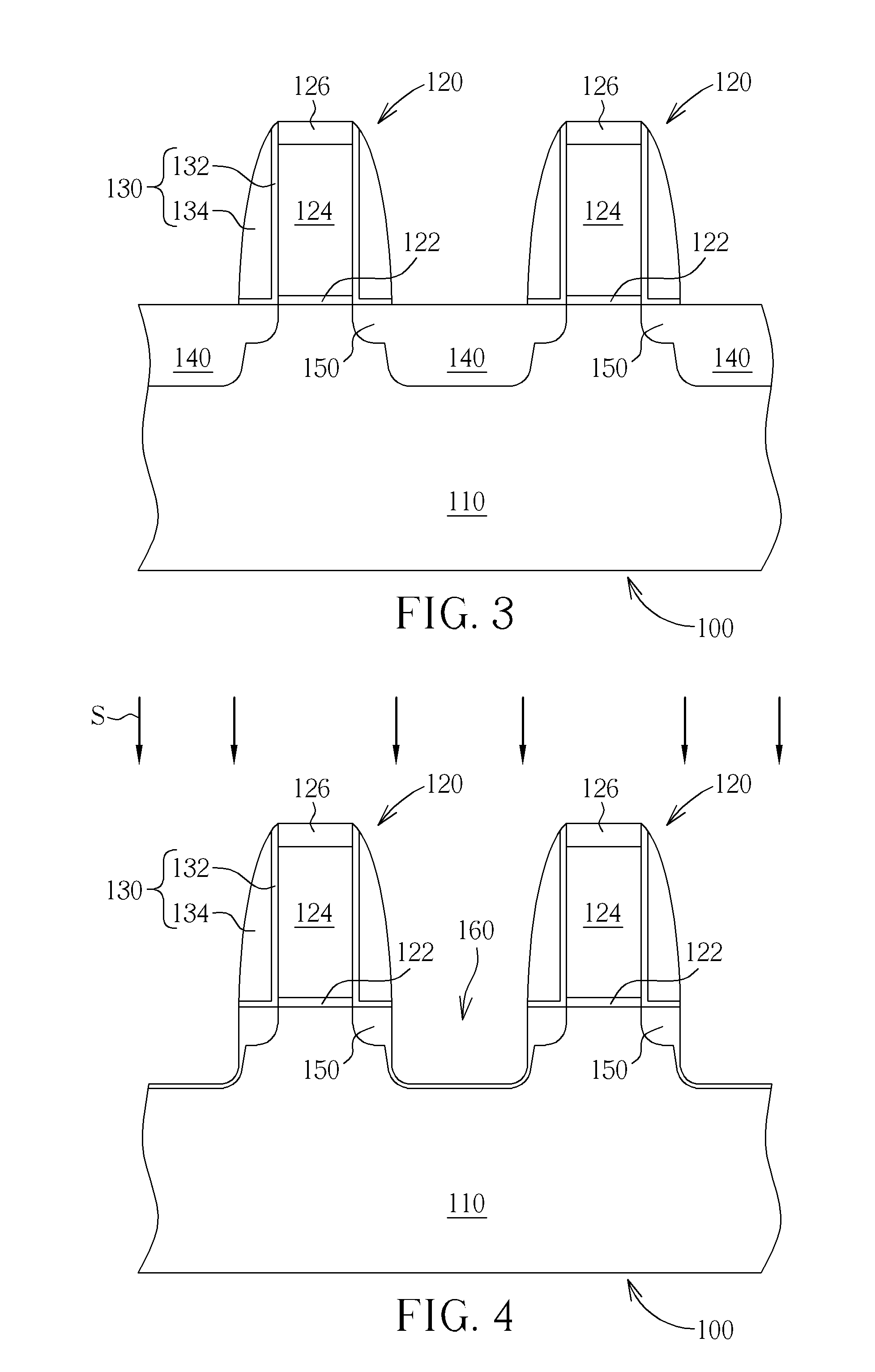
[0016]FIGS. 3-6 are schematic, cross-sectional diagrams illustrating a semiconductor process applying epitaxial technology in accordance with a preferred embodiment of the present invention. As shown in FIG. 3, a substrate 110 is provided, in which the substrate 110 can be a doped or undoped single crystal silicon. A doped well and an insulating layer are formed sequentially on the substrate 110 to provide an insulation between adjacent devices or transistors (not shown). The insulating layer can be a trench insulation structure, and the fabrication thereof can be obtained by etching a recess and then depositing an oxide layer within the recess. The details which are not explained herein for the sake of brevity. In one example, the trench insulation structure can be a shallow trench isolation structure (STI), but not limited thereto.

[0017]A gate structure 120 is formed on the substrate 110. The gate structure 120 includes a gate dielectric layer 122 and a gate electrode 124. The fab...


PUM


Abstract

A semiconductor process is disclosed. The semiconductor process includes the steps of: providing a substrate having a specific area defined thereon; and performing an etch process by using an etchant comprising H2O2 to etch the specific area for forming a recess.

Description

BACKGROUND OF THE INVENTION[0001]1. Field of the Invention[0002]The present invention relates to a semiconductor process, and more particularly, to a semiconductor process of using an etchant including H2O2 for etching a recess.[0003]2. Description of the Prior Art[0004]For decades, chip manufacturers have made metal-oxide-semiconductor (MOS) transistors faster by making them smaller. As the semiconductor processes advance to very deep sub micron era such as 65-nm node or beyond, how to increase the driving current for MOS transistors has become a critical issue.[0005]In order to improve device performance, crystal strain technology has been developed. Crystal strain technology is becoming more and more attractive as a means for getting better performance in the field of CMOS transistor fabrication. Putting a strain on a semiconductor crystal alters the speed at which charges move through that crystal. Strain makes CMOS transistors work better by enabling electrical charges, such as...

Claims


Application Information

Patent Timeline
Patent Type & Authority Applications(United States)
IPC IPC(8): H01L21/335H01L21/306H01L21/20
CPCH01L21/30608H01L29/7848H01L29/78H01L29/66636
Inventor WU, CHUN-YUANYEH, CHIU-HSIENCHIEN, CHIN-CHENG
Owner UNITED MICROELECTRONICS CORP
Why Eureka
Try Eureka