System and method for input pin ESD protection with floating and/or biased polysilicon regions

a polysilicon region and polysilicon technology, applied in the field of integrated circuits, can solve the problems of difficult reducing breakdown voltage, difficult to reduce breakdown voltage, and difficult to use devices small, so as to improve the protection technique of input pins, reduce the breakdown voltage of certain protection transistors, and improve the effect of input pin esd protection

Active Publication Date: 2012-01-05
SEMICON MFG INT (SHANGHAI) CORP +1
View PDF1 Cites 2 Cited by
  • Summary
  • Abstract
  • Description
  • Claims
  • Application Information

AI Technical Summary

Benefits of technology

[0011]Embodiments of the present invention provide many benefits over conventional techniques. For example, the present technique provides an easy to use system and method. According to some embodiments, the system and method are compatible with conventional technology. Some embodiments of the present invention improve the input pin ESD protection technique. For example, the junction breakdown voltages of certain protection transistors are lowered. In another example, the protection transistors enter the breakdown mode in the off state and thus prevent or reduce damages to the core transistors from ESD stress. Certain embodiments of the present invention can effectively delay the time when the ESD stress current reaches the gate regions. For example, the channels formed under the polysilicon regions have significant resistance, which can lengthen the current paths. Some embodiments of the present invention comply with the ESD design rule. For example, to dissipate significant heat generated by high-density ESD current, the ESD design rule often allows relatively large spacing between the gate regions and drain contacts. In another example, the spacing is equal to or longer than 1.72 μm. Accordingly, the polysilicon regions can be inserted to the drain regions of the protection transistors in order to increase lengths of the current paths and raise the drain resistance without violating the ESD design rule. Certain embodiments of the present invention provide junction doping profiles between LDD regions and pocket implant regions related to floating and / or biased polysilicon regions, which is steeper than junction doping profiles between LDD regions and pocket implant regions for protection transistors. Some embodiments of the present invention significantly lower junction breakdown voltage of secondary transistors until the primary ESD transistors are fully functional to protect the input pin. For example, the secondary transistors with lowered junction breakdown voltage can effectively limit the voltage or current of the protected system until the primary ESD transistors are fully operational for protection. Some embodiments of the present invention use certain protection transistors that are the same as the protected transistors, such as the core transistors. Depending upon the embodiment, one or more of these benefits may be achieved. These and other benefits will be described in more detail throughout the present specification and more particularly below.

Problems solved by technology

An IC fabrication facility can cost hundreds of millions, or even billions, of dollars.
Making devices smaller is very challenging, as a given process and / or device layout often work down to only a certain feature size.
An effective protection often requires lowering breakdown voltages of these transistors, but reducing the breakdown voltages can be difficult.
Conventionally, an ESD implant may be used for adjusting the breakdown voltages, but the ESD implant often increases fabrication complexity with limited effectiveness.

Method used


Image

  • System and method for input pin ESD protection with floating and/or biased polysilicon regions
  • System and method for input pin ESD protection with floating and/or biased polysilicon regions
  • System and method for input pin ESD protection with floating and/or biased polysilicon regions

Examples


Embodiment Construction

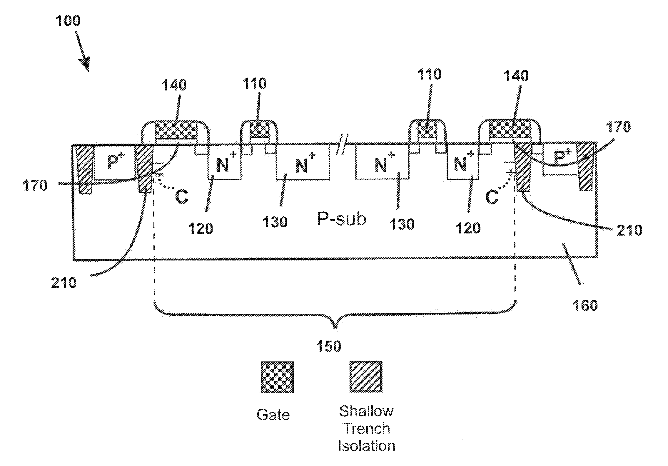
[0022]Embodiments of the present invention relate to integrated circuits. More particularly, embodiments of the invention provide a system and method for electrostatic discharge (ESD) protection with floating and / or biased polysilicon regions. Merely by way of example, the invention has been applied to input pins. But it would be recognized that the invention has a much broader range of applicability.

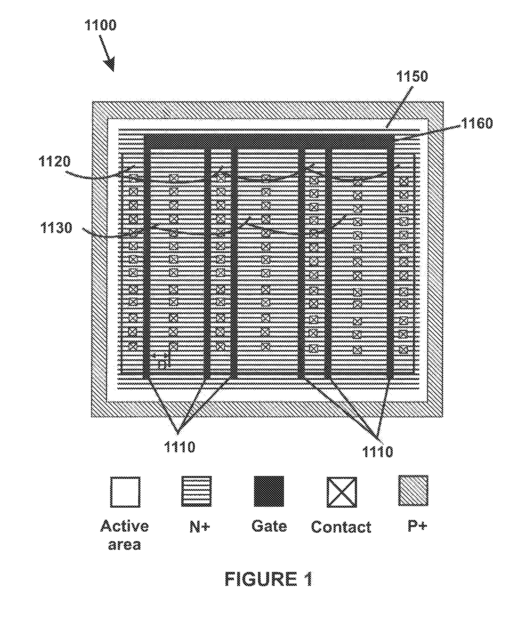
[0023]FIG. 1 is a simplified conventional system for electrostatic discharge protection. The system 1100 includes gate regions 1110, source regions 1120, drain regions 1130, an active area 1150, and a polysilicon region 1160. The gate regions 1110, the source regions 1120, and the drain regions 1130 are used to form I / O transistors in the active area 1150. The gate regions are electrically shorted to each other by the polysilicon region 1160, and the polysilicon region 1160 is located completely outside the active area 1150.

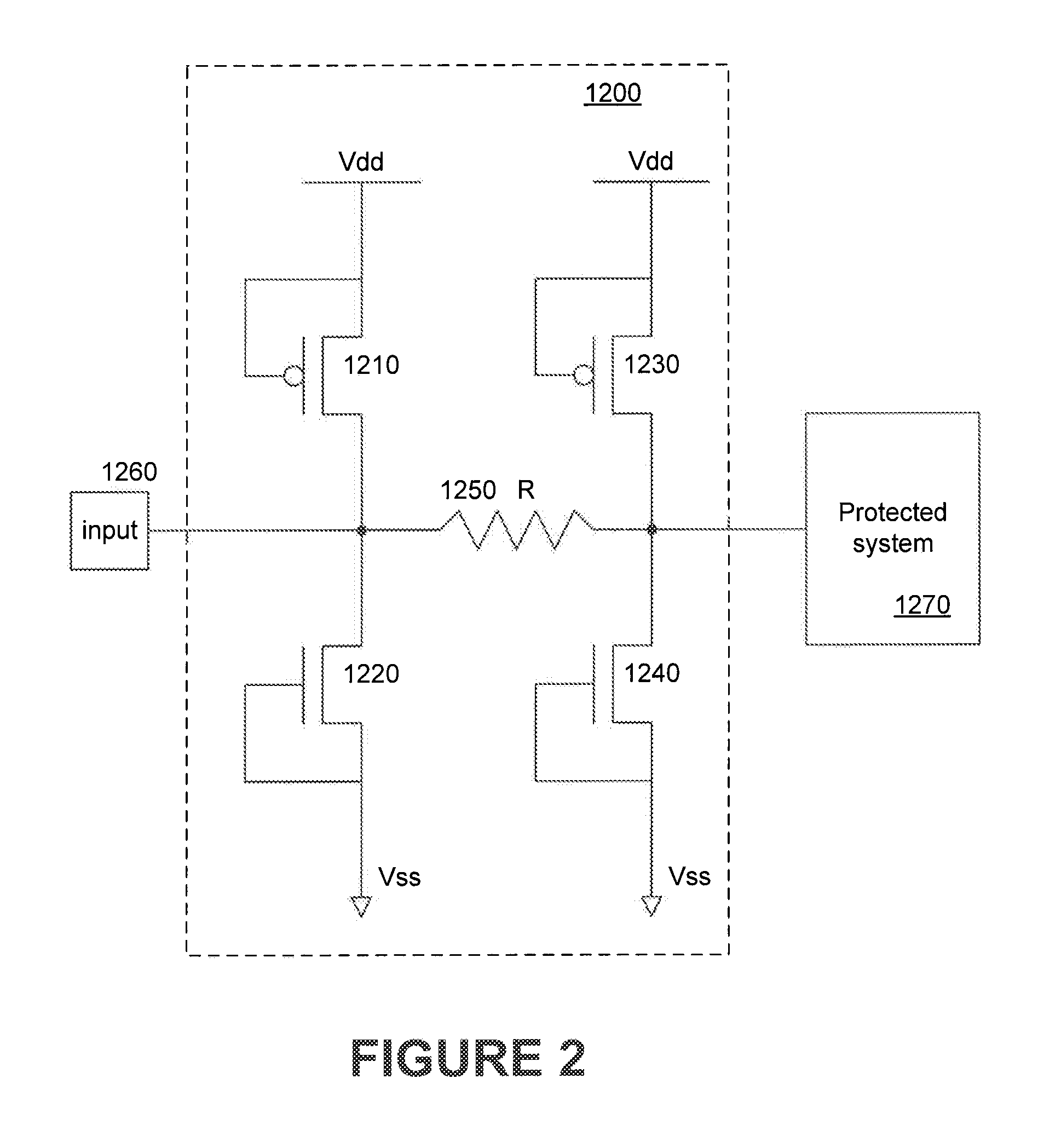
[0024]FIG. 2 is a simplified system for electrostatic discharge...


PUM


Abstract

A system and method for electrostatic discharge protection. The system includes a first transistor including a first drain, a second transistor including a second drain, and a resistor including a first terminal and a second terminal. The first terminal is coupled to the first drain and the second drain. Additionally, the system includes a third transistor coupled to the second terminal and a protected system. The third transistor includes a first gate, a first dielectric layer located between the first gate and a first substrate, a first source, and a third drain. The protected system includes a fourth transistor, and the fourth transistor includes a second gate, a second dielectric layer located between the second gate and a second substrate, a second source, and a fourth drain.

Description

CROSS-REFERENCES TO RELATED APPLICATIONS[0001]This application claims priority to Chinese Patent Application No. 200910247495.7, filed Dec. 29, 2009, which is commonly owned and incorporated by reference herein for all purposes.[0002]This application is related to U.S. patent application Ser. No. 11 / 517,546, filed Sep. 6, 2006, and to U.S. patent application Ser. No. 11 / 550,529, filed Oct. 18, 2006, now U.S. Pat. No. 7,642,602, which are commonly assigned and incorporated by reference herein for all purposes.BACKGROUND OF THE INVENTION[0003]Embodiments of the present invention generally relate to integrated circuits. More particularly, embodiments of the invention provide a system and method for electrostatic discharge (ESD) protection with floating and / or biased polysilicon regions. Merely by way of example, embodiments of the invention have been applied to input pins. But it would be recognized that the invention has a much broader range of applicability.[0004]Integrated circuits ...

Claims


Application Information

Patent Timeline
Patent Type & Authority Applications(United States)
IPC IPC(8): H01L23/60
CPCH01L27/027
Inventor SU, TING CHIEHJENG, MIN CHIELIAO, CHIN CHANGHUANG, JUN CHENG
Owner SEMICON MFG INT (SHANGHAI) CORP
Why Eureka
Try Eureka