Production method of n-type sic single crystal, n-type sic single crystal obtained thereby and application of same
a production method and single crystal technology, applied in the direction of crystal growth process, polycrystalline material growth, conductors, etc., can solve the problems of affecting the inherent characteristics of sic single crystal, and achieve low specific resistance, low specific resistance, and low specific resistance
- Summary
- Abstract
- Description
- Claims
- Application Information
AI Technical Summary
Benefits of technology
Problems solved by technology
Method used
Image
Examples
example 1
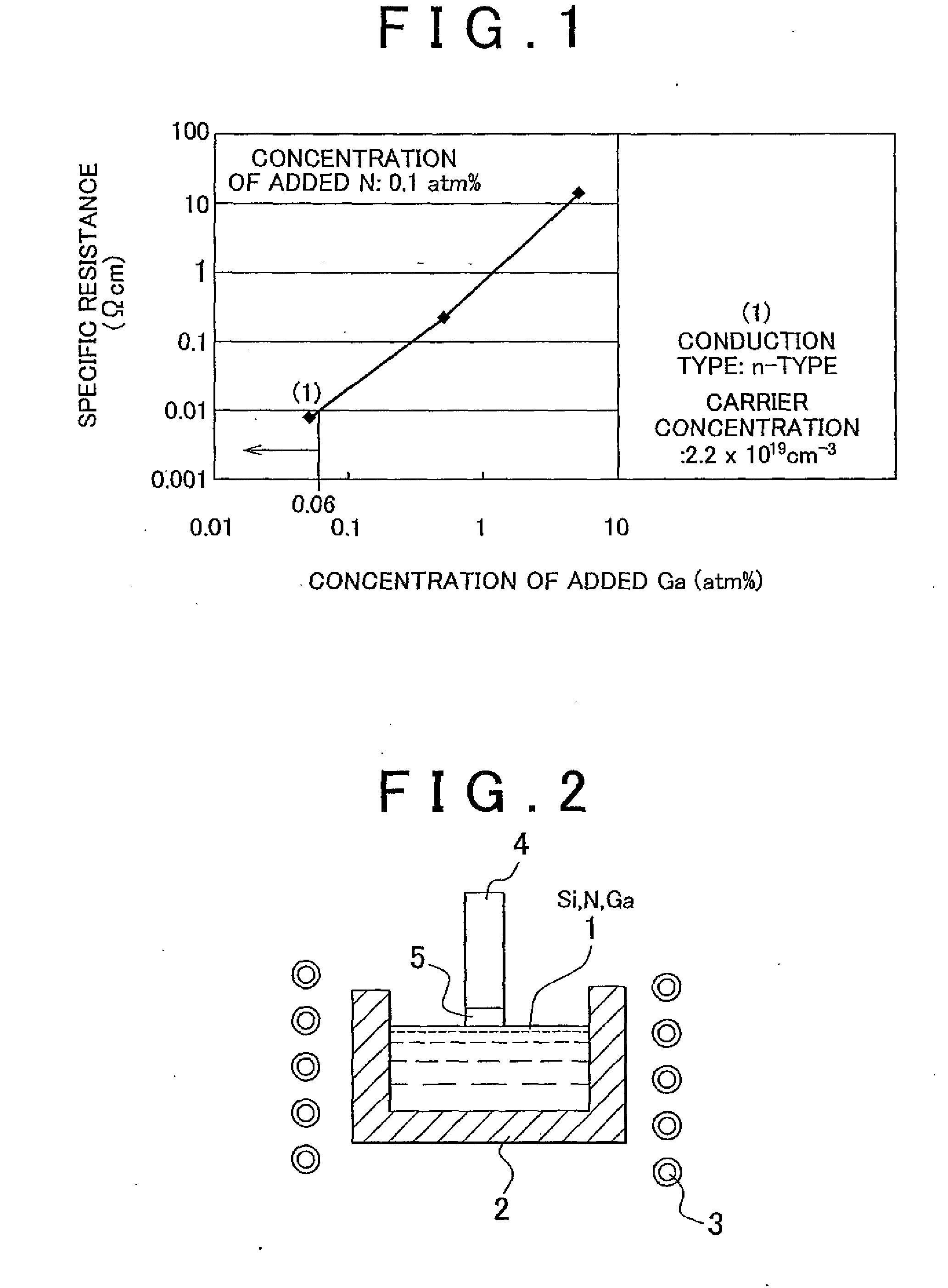
[0040]Crystal growth was carried out using the apparatus shown in FIG. 2. The raw material consists of 60 atm % of Si, 40 atm % of Cr, 0.1 atm % of N (the entire amount was supplied in the form of nitrogen gas) and 0.05 atm % of Ga to the SiC respectively were put in a graphite crucible. A seed crystal of 4H—SiC single crystal was immersed in a melt heated to a growth temperature of 2010° C. for about 8 hours to induce crystal growth. The resulting SIC single crystal was evaluated by the Hall measurement. The results are summarized in FIG. 1 and Table 1. In addition, temperature characteristics of specific resistance were evaluated. Those results are summarized in FIGS. 7A and 7B. FIG. 7A shows specific resistance temperature characteristics over a wide temperature range, while FIG. 7B shows specific resistance temperature characteristics over a narrow temperature range.
example 2
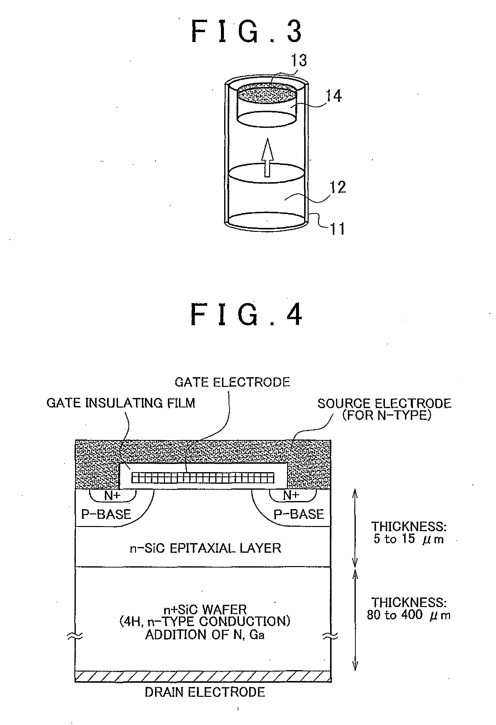
[0046]A cross-sectional schematic diagram of a switching device that uses n-type SiC single crystal obtained according to the invention as an n+ wafer is shown in FIG. 4. Incidentally, “n+” shown in FIG. 4 indicates that the wafer is of n-type conduction and has a high concentration of dopant.
example 3
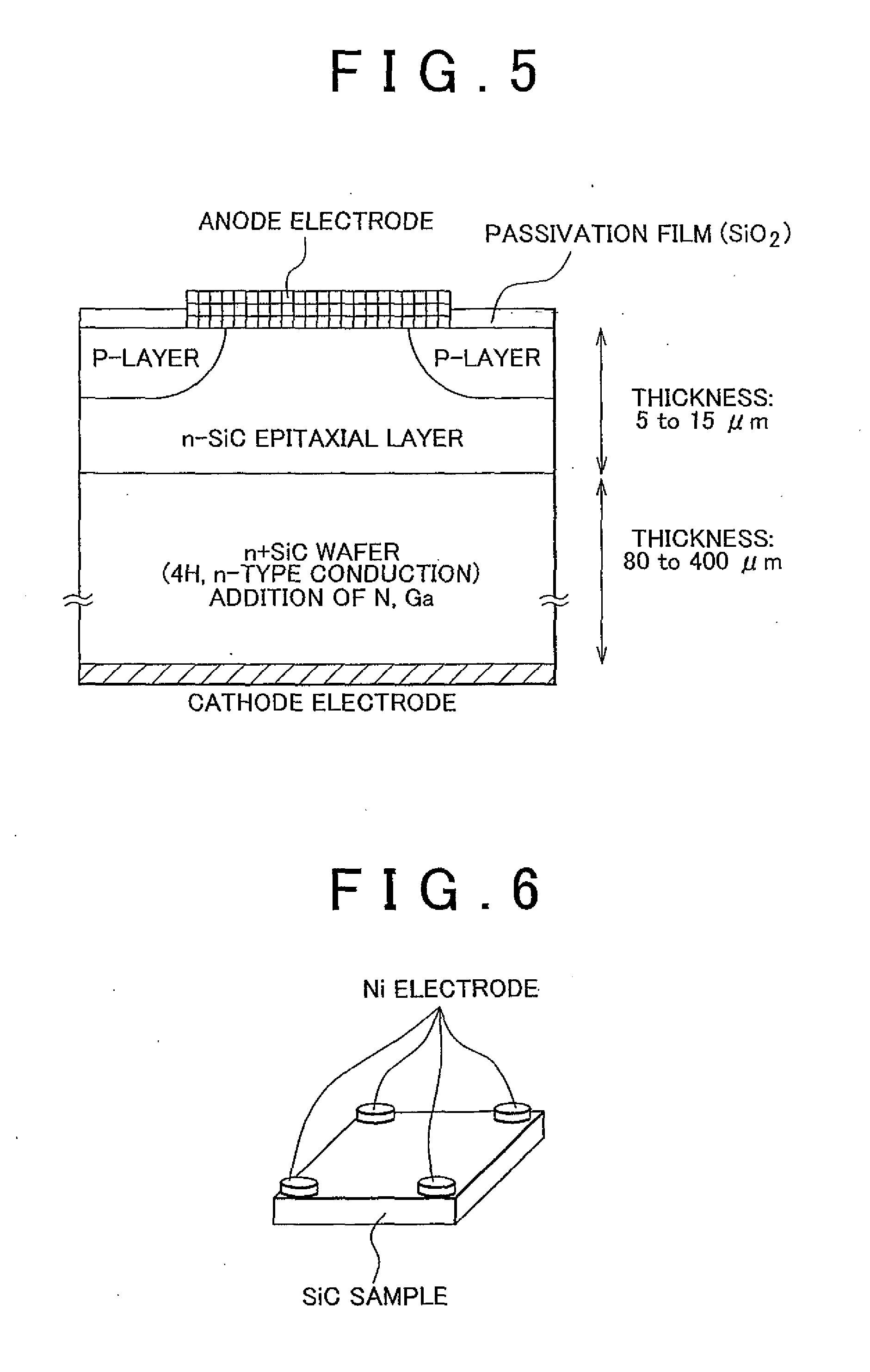
[0047]A cross-sectional schematic diagram of a Schottky barrier diode (SBD) that uses an n-type SiC single crystal obtained according to the invention as an n+ wafer is shown in FIG. 5. Incidentally, “n+” shown in FIG. 5 indicates that the wafer is of n-type conduction and has a high concentration of dopant.
[0048]According to the SiC single crystal production method of the invention, n-type SiC single crystal can be obtained that has low specific resistance as well as low carrier concentration that were unable to be previously realized, thereby enabling the production of n-type SiC single crystal with favorable reproducibility.
PUM
| Property | Measurement | Unit |
|---|---|---|
| band gap | aaaaa | aaaaa |
| band gap | aaaaa | aaaaa |
| resistivity | aaaaa | aaaaa |
Abstract
Description
Claims
Application Information
 - R&D
- Intellectual Property
- Life Sciences
- Materials
- Tech Scout
- Unparalleled Data Quality
- Higher Quality Content
- 60% Fewer Hallucinations
Browse by: Latest US Patents, China's latest patents, Technical Efficacy Thesaurus, Application Domain, Technology Topic, Popular Technical Reports.
© 2025 PatSnap. All rights reserved.Legal|Privacy policy|Modern Slavery Act Transparency Statement|Sitemap|About US| Contact US: help@patsnap.com


