Optical sensor and device therewith, and method for the production thereof
- Summary
- Abstract
- Description
- Claims
- Application Information
AI Technical Summary
Benefits of technology
Problems solved by technology
Method used
Image
Examples
example
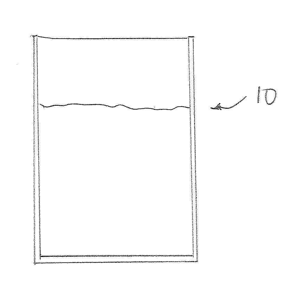
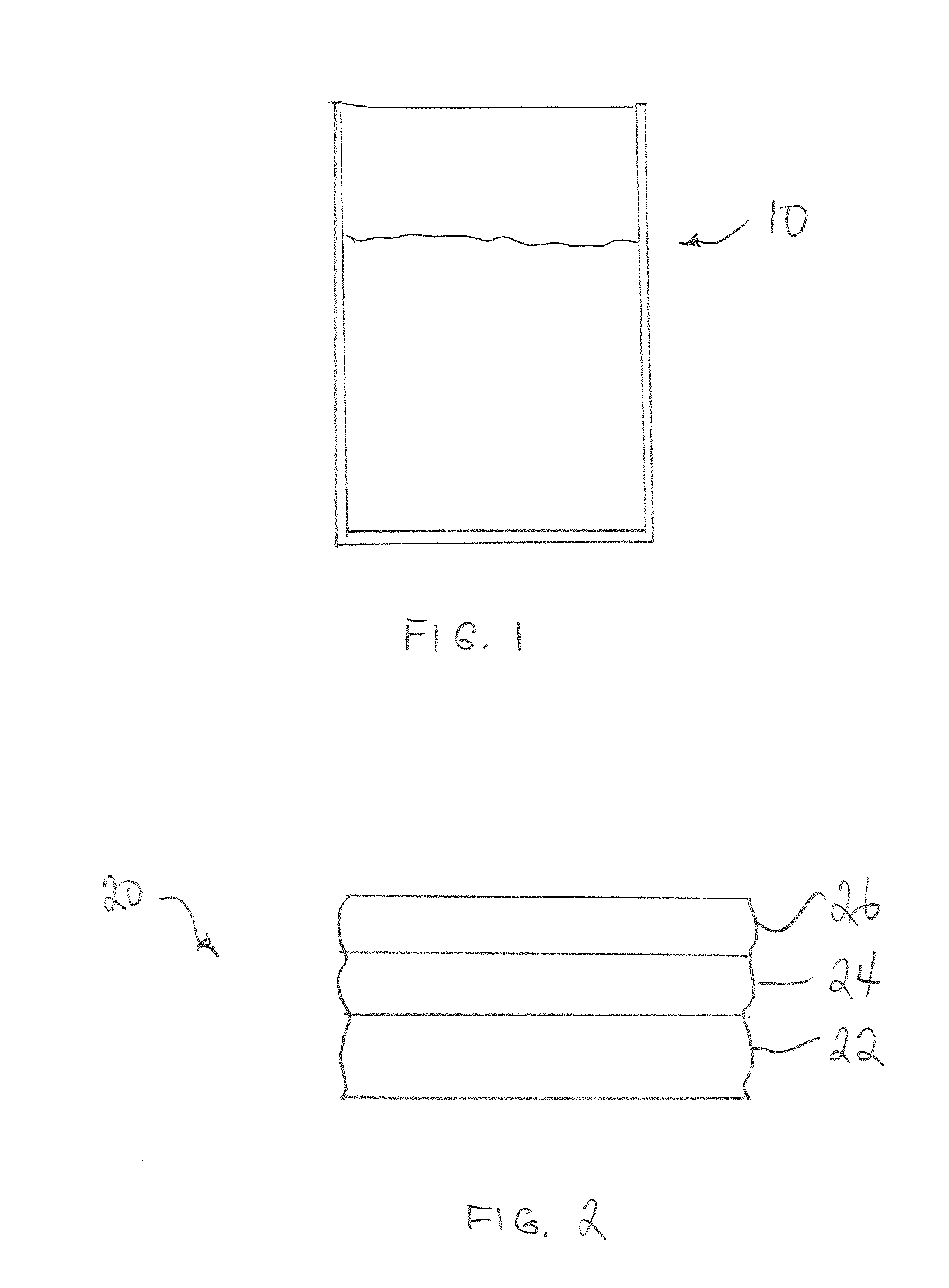
Plastic containers 10 (Cultibag RM, Sartorius Stedim Biotech GmbH, Gottingen / Volume: 10 l) are equipped with the optical sensors 20 according to the invention (pH-Sensors Type HP8, Presens GmbH, Regensburg) on a polycarbonate cap. The gold layer 26 is applied by means of magnetron sputtering (EMITECH K550 sputter coater and gold target; parameters: pressure: 1 Pa atmospheric pressure, sputtering current: 50 mA, sputtering time: 5 minutes), with the layer thickness being 150 nm. The sensors 20 are applied centrally in the interior of the container and directly next to sensors of the same type without a gold layer, with the sensor chemicals facing the center of the container. The device 10 is subsequently filled with 10 l of air or nitrogen (N2) and packaged in black, light-opaque PE-bags. Thereupon there is gamma-irradiation at 5.8 kGy and 26.2 kGy (Co-60 source, Beta-Gamma-Service GmbH & Co. KG, Wiehl).
After irradiation, the sensors 20 are removed from the containers and measured by...
PUM
| Property | Measurement | Unit |
|---|---|---|
| Thickness | aaaaa | aaaaa |
| Thickness | aaaaa | aaaaa |
| Pressure | aaaaa | aaaaa |
Abstract
Description
Claims
Application Information
 - R&D
- Intellectual Property
- Life Sciences
- Materials
- Tech Scout
- Unparalleled Data Quality
- Higher Quality Content
- 60% Fewer Hallucinations
Browse by: Latest US Patents, China's latest patents, Technical Efficacy Thesaurus, Application Domain, Technology Topic, Popular Technical Reports.
© 2025 PatSnap. All rights reserved.Legal|Privacy policy|Modern Slavery Act Transparency Statement|Sitemap|About US| Contact US: help@patsnap.com


