
Copper Foil for Printed Circuit

a technology of printed circuits and copper foils, applied in the direction of instruments, heat measurement, cores/yokes, etc., can solve the problems of more severe treatment requirements in the production process of printed circuits, and achieve the effect of further reducing size and higher integration

Active Publication Date: 2011-10-27
JX NIPPON MINING & METALS CORP
View PDF5 Cites 28 Cited by
  • Summary
  • Abstract
  • Description
  • Claims
  • Application Information

AI Technical Summary

Benefits of technology

The present invention provides a copper foil for a printed circuit with a smooth surface and reduced roughening treatment. The copper foil has a layer of copper-cobalt-nickel alloy plating with dendritic particles and a roughened layer based on copper-cobalt-nickel alloy plating. The roughened layer has a specific composition and a zinc-nickel alloy plated layer can be additionally formed on the roughened layer. The copper foil can be bonded to a resin substrate to produce a copper clad laminate. The invention can provide a solution for the demand for smoother and more uniform treatment in printed circuit production.

Problems solved by technology

There are even more severe demands for the treatment in a production process of printed circuits.

Method used


Image

  • Copper Foil for Printed Circuit
  • Copper Foil for Printed Circuit
  • Copper Foil for Printed Circuit

Examples


examples

[0101]The Examples and Comparative Examples of the present invention are now explained. These Examples are merely illustrative, and the present invention shall in no way be limited thereby. In other words, various modifications and other embodiments based on the technical spirit claimed in the claims shall be included in the present invention as a matter of course.

example

[0102]Roughening treatment was performed to a rolled copper foil by way of copper-cobalt-nickel alloy plating within the range of the following conditions. After adhering 17 mg / dm2 of copper, 2000 μg / dm2 of cobalt and 500 μg / dm2 of nickel, the copper foil was water washed, and a cobalt-nickel alloy plated layer was formed thereon. Here, the deposited mass of cobalt was 800 to 1400 μg / dm2, and the deposited mass of nickel was 400 to 600 μg / dm2.

[0103]The used bath composition and plating conditions were as follows.

[Bath Composition and Plating Conditions]

(A) Roughening Treatment (Cu—Co—Ni Alloy Plating)

[0104]Cu: 15.5 g / liter

[0105]Co: 6 g / liter

[0106]Ni: 11 g / liter

[0107]pH: 2.5

[0108]Temperature: 30° C.

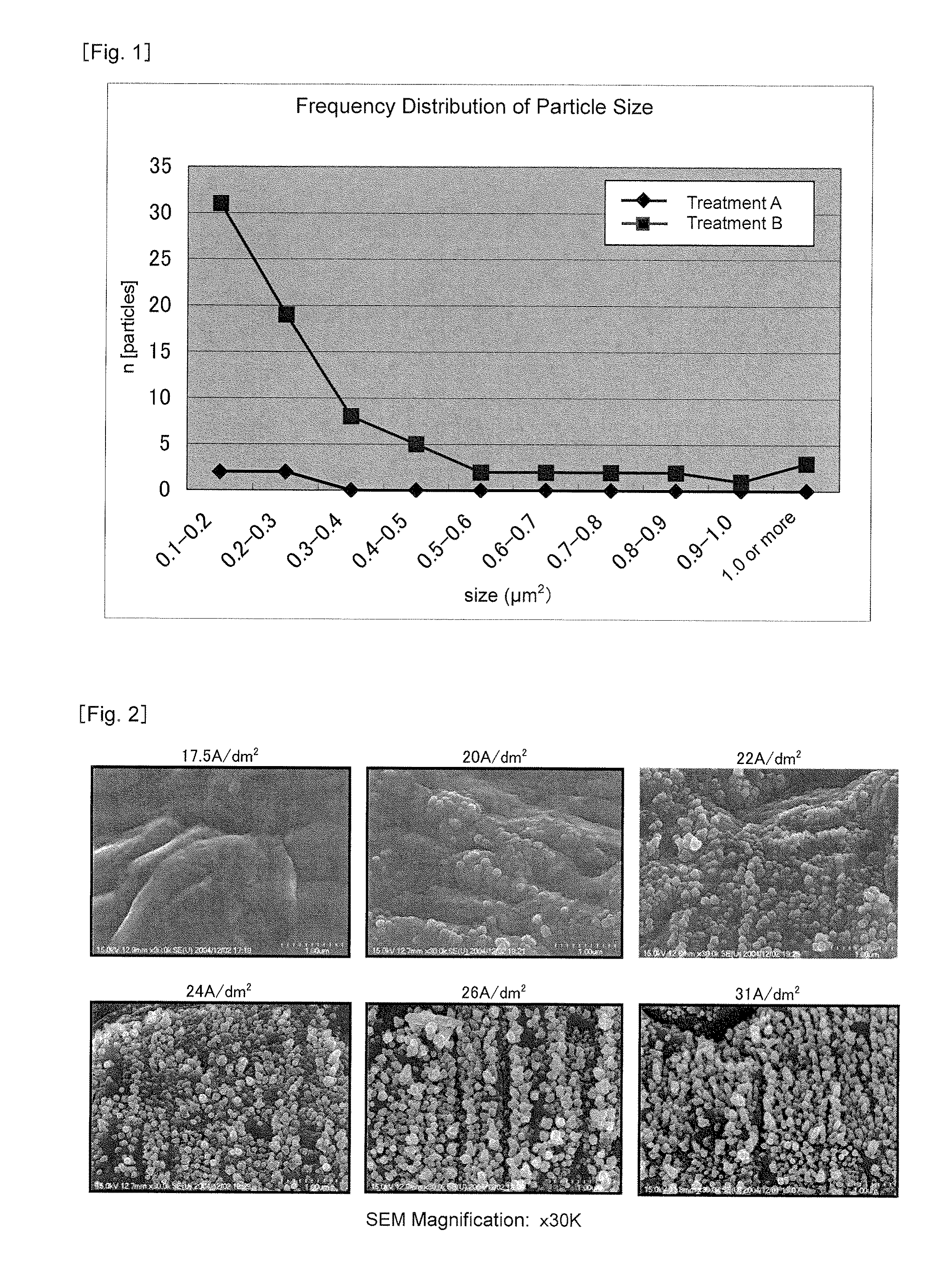
[0109]Current Density Dk: 20 A / dm2

[0110]Time: 2 seconds

[0111]Deposited mass of copper: 17 mg / dm2

[0112]Deposited mass of cobalt: 2000 μg / dm2

[0113]Deposited mass of nickel: 500 μg / dm2


PUM

PropertyMeasurementUnit
areaaaaaaaaaaa
areaaaaaaaaaaa
widthaaaaaaaaaa

Abstract

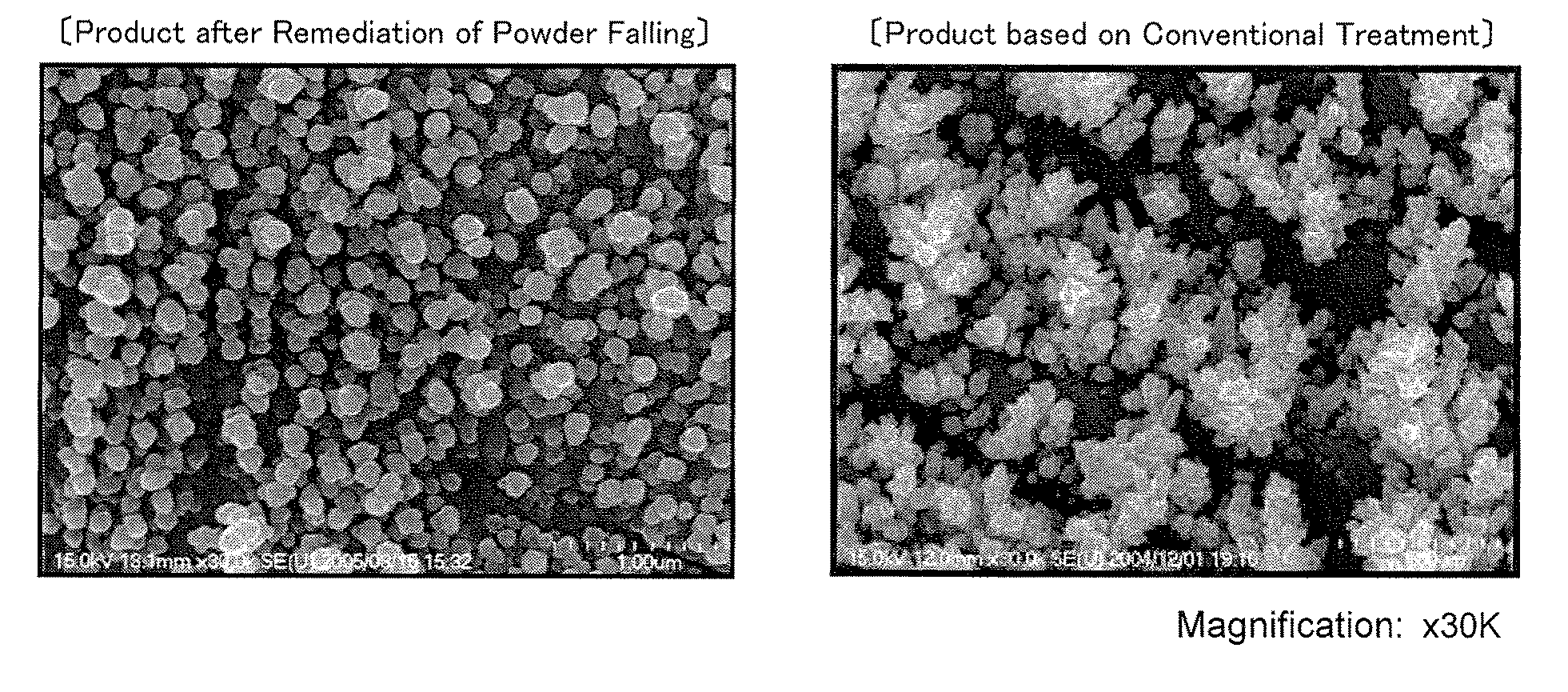
Provided is a copper foil for a printed circuit with an electrodeposited ternary-alloy layer composed of copper, cobalt and nickel formed on a surface of the copper foil, wherein the electrodeposited layer comprises dendritic particles grown on the copper foil surface, and the entire surface of the copper foil is covered with particles having an area as seen from above the copper foil surface of 0.1 to 0.5 μm2 at a density of 1000 particles / 10000 μm2 or less, particles exceeding 0.5 μm2 at a density of 100 particles / 10000 μm2 or less, and particles less than 0.1 μm2 as the remainder. Roughening particles formed dendritically in a roughening treatment based on copper-cobalt-nickel alloy plating are inhibited from shedding from the copper foil surface, and the phenomenon known as powder falling and uneven treatment are thereby inhibited.

Description

TECHNICAL FIELD[0001]The present invention relates to a copper foil for a printed circuit, and in particular relates to a copper foil for a printed circuit capable of reducing the powder falling and uneven treatment of a roughened layer obtained by performing copper-cobalt-nickel alloy plating to the surface of a copper foil. The copper foil for a printed circuit of the present invention can be suitably applied, for example, to a fine pattern printed circuit and a FPC (Flexible Printed Circuit) for magnetic head.BACKGROUND ART[0002]Copper and copper alloy foil (hereinafter collectively referred to as “copper foil”) have contributed significantly to the development of the electric / electronic industry and, in particular, are indispensible as a printed circuit material. A copper foil for a printed circuit is generally prepared as follows. In order to produce a copper clad laminate, copper foil is laminated and bonded to a base material such as a synthetic resin board or film with an ad...

Claims


Application Information

Patent Timeline
Patent Type & Authority Applications(United States)
IPC IPC(8): B32B15/08B32B15/01
CPCC25D3/58Y10T428/12861C25D7/0614H05K3/384H05K2201/0355H05K2203/0307H05K2203/0723C25D1/04Y10T428/12514Y10T428/1291Y10T428/12063Y10T428/12049Y10T428/12458Y10T428/12868C25D5/00C25D5/605
Inventor ARAI, HIDETAHIGUCHI, NAOKI
Owner JX NIPPON MINING & METALS CORP
Learn More