
Mach-zehnder interferometer type optical modulator

Active Publication Date: 2011-09-29
SUMITOMO ELECTRIC IND LTD
View PDF2 Cites 25 Cited by
  • Summary
  • Abstract
  • Description
  • Claims
  • Application Information

AI Technical Summary

Benefits of technology

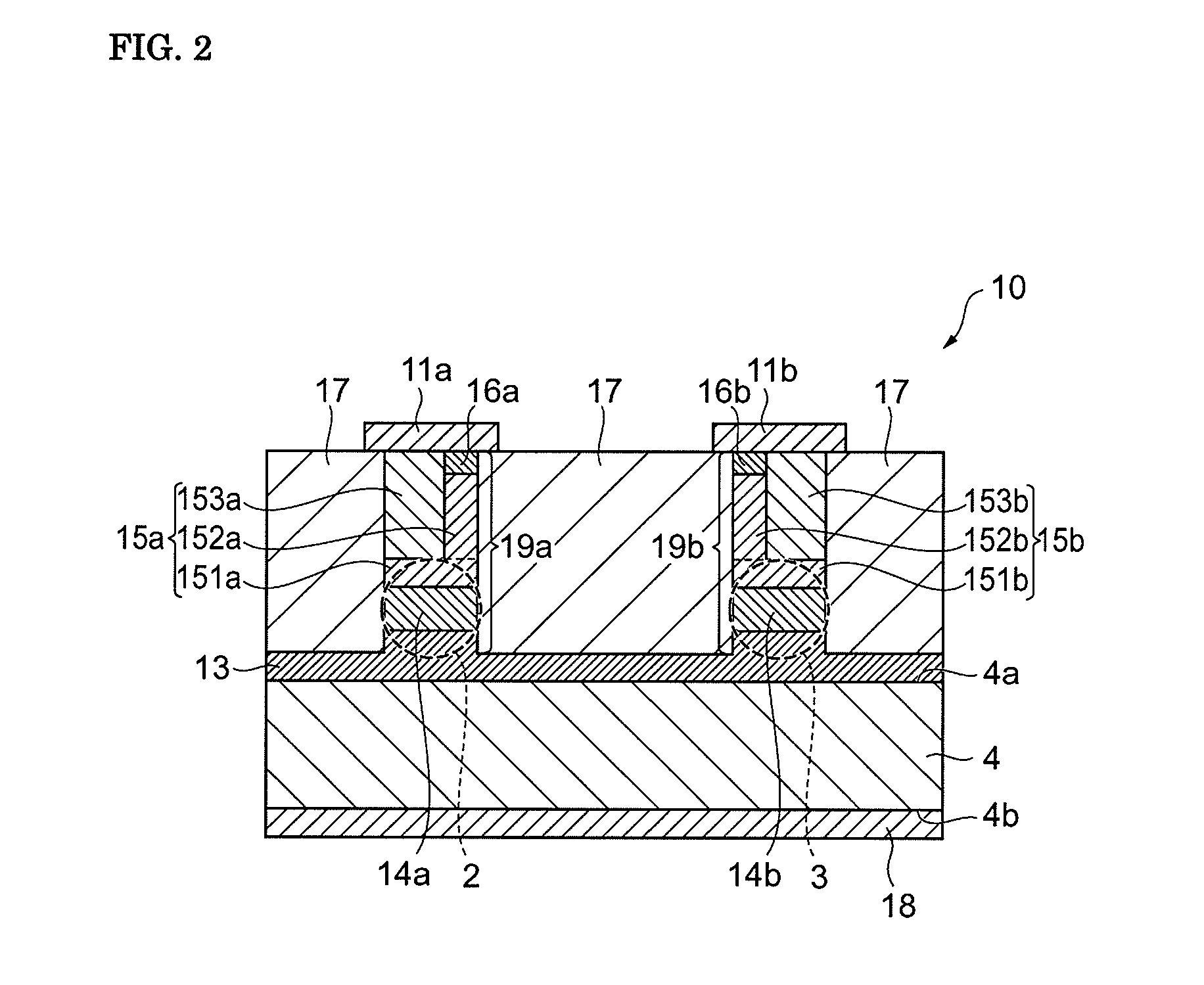
[0014]According to the Mach-Zehnder interferometer type optical modulator, the cladding layer of the first optical waveguide structure of the phase shifting section includes the first section, the second section, and the third section. The first section composed of a p-type semiconductor is disposed on the core layer and a pin structure is formed by the core layer sandwiched between the p-type first section and the n-type semiconductor section. The second section composed of a p-type semiconductor is disposed on the first section and transfers an electrical signal applied to the first anode electrode to the first section. The third section is also formed on the first section by being juxtaposed to the second section. The cladding layer of the second optical waveguide structure of the phase shifting section includes the fourth section, the fifth section, and the sixth section. The fourth section composed of a p-type semiconductor is disposed on the core layer and a pin structure is formed by the core layer sandwiched between the p-type fourth section and the n-type semiconductor section. The fifth section composed of a p-type semiconductor is disposed on the fourth section and transfers an electrical signal applied to the second anode electrode to the fourth section. The sixth section is also formed on the fourth section by being juxtaposed to the fifth section. Since the third and sixth sections are composed of an undoped semiconductor, the optical absorption loss can be reduced when compared with the second and fifth sections composed of a p-type semiconductor. According to this Mach-Zehnder interferometer type optical modulator, the optical absorption loss in the phase shifting section can be reduced compared to the case where all of the cladding layers are composed of a p-type semiconductor.
[0018]Since no electric field is applied to the core layers of the first and second optical waveguides excluding the phase shifting section, the input optical coupler, and the output optical coupler, there is no need to impart electrical conductivity to the cladding layers. Accordingly, all regions other than the seventh sections inevitably formed together with the first sections of the cladding layers of the phase shifting section during manufacturing can be made of an undoped material so that the optical absorption loss and the like that occur in the first and second optical waveguides excluding the phase shifting section, the input optical coupler, and the output optical coupler can be reduced.
[0019]The Mach-Zehnder interferometer type optical modulator may further include a first p-type contact layer disposed on the second section and having a dopant concentration higher than that in the second section, and a second p-type contact layer disposed on the fifth section and having a dopant concentration higher than that in the fifth section. In this manner, electrical signals applied to the first anode electrode on the first p-type contact layer can be efficiently transmitted to the first and second sections. Similarly, electrical signals applied to the second anode electrode on the second p-type contact layer can be efficiently transmitted to the fourth and fifth sections.
[0020]The first p-type contact layer of the Mach-Zehnder interferometer type optical modulator may extend across the second section and the third section. The second p-type contact layer of the Mach-Zehnder interferometer type optical modulator may extend across the fifth section and the sixth section. In this manner, the contact area between the first anode electrode and the first p-type contact layer can be increased and the contact resistance can be reduced. Similarly, the contact area between the second anode electrode and the second p-type contact layer can be increased and the contact resistance can be reduced. As a result, the device resistance is decreased and electrical signals can be transferred to the fourth and fifth sections with a lower voltage. In other words, the Mach-Zehnder interferometer type optical modulator can be operated at a lower voltage and a lower power consumption.

Problems solved by technology

Moreover, since the electrical resistance between the optical waveguides is small, leakage current occurs between the optical waveguides.
Accordingly, it is difficult to decrease the optical absorption loss of guided light and increase the modulation rate by taking the structure such as this Mach-Zehnder interferometer type optical modulator.

Method used


Image

  • Mach-zehnder interferometer type optical modulator
  • Mach-zehnder interferometer type optical modulator
  • Mach-zehnder interferometer type optical modulator

Examples


first embodiment

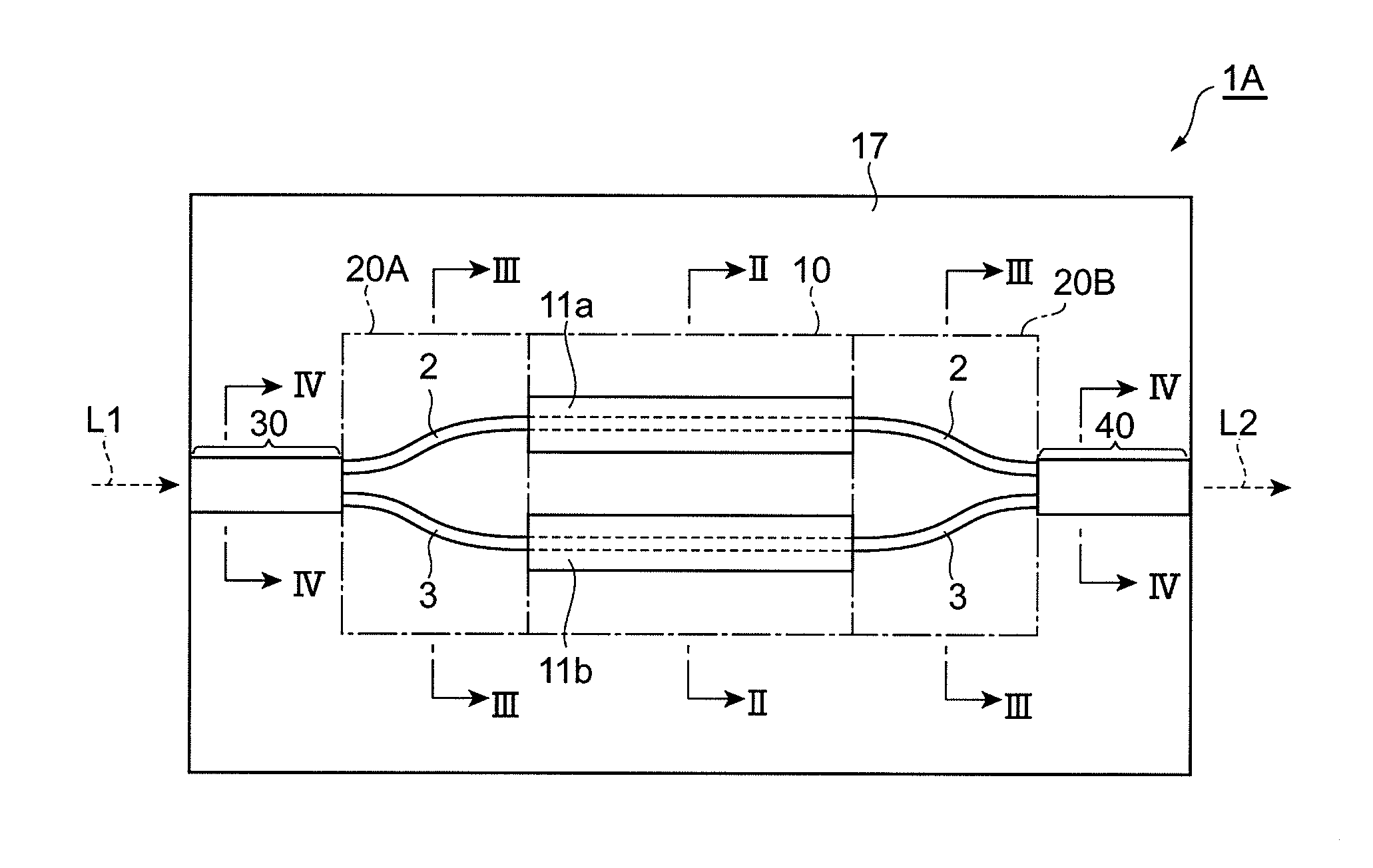
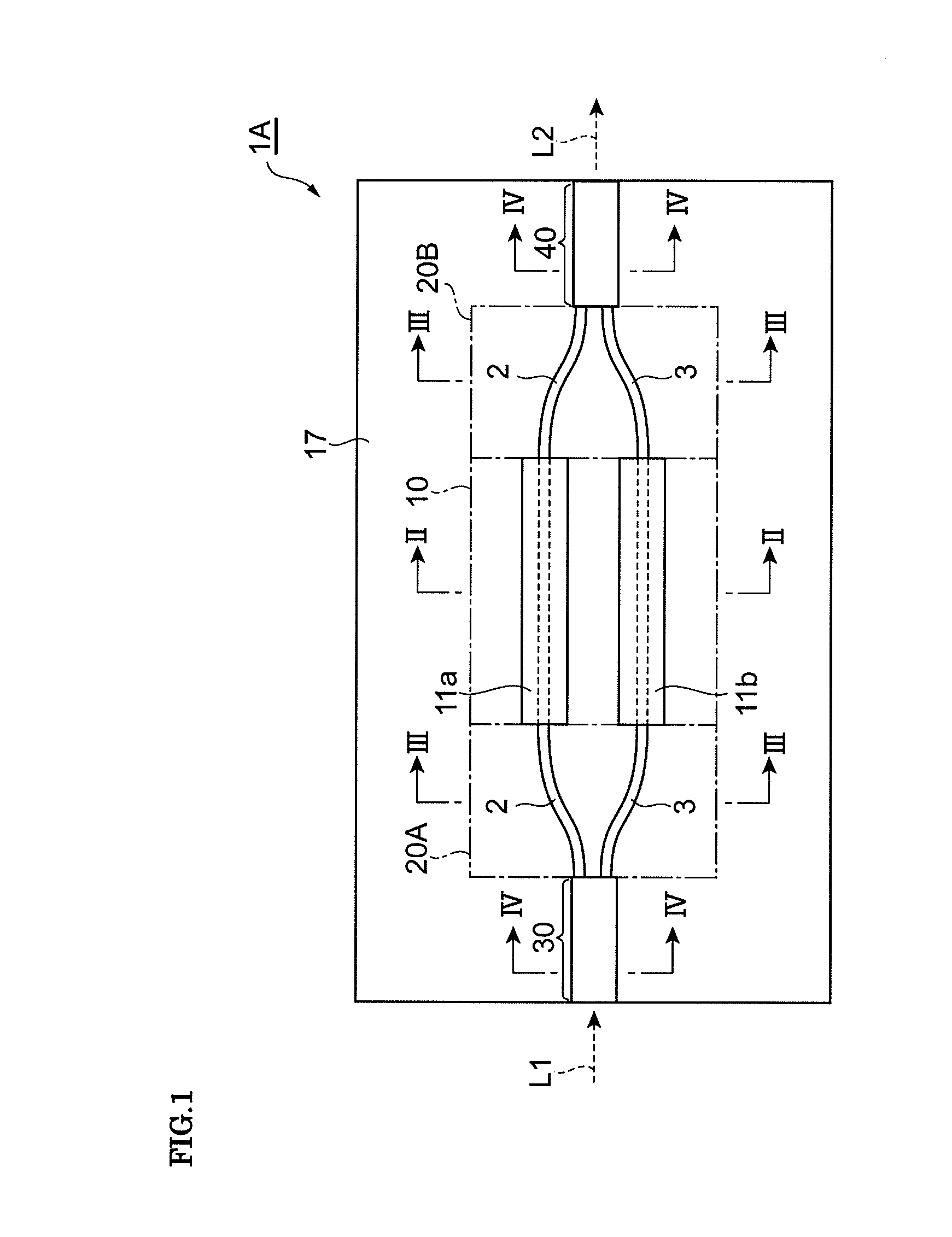
[0040]FIGS. 1 to 4 are diagrams showing a structure of a Mach-Zehnder interferometer type optical modulator 1A according to a first embodiment. FIG. 1 is a plan view showing a structure of the Mach-Zehnder interferometer type optical modulator 1A. FIGS. 2, 3, and 4 are cross-sectional views of the Mach-Zehnder interferometer type optical modulator 1A shown in FIG. 1 taken along line II-II, line III-III, and line IV-IV, respectively.

[0041]Referring to FIG. 1, the Mach-Zehnder interferometer type optical modulator 1A of this embodiment includes a phase shifting section 10, waveguiding sections 20A and 20B, an input optical coupler 30, and an output optical coupler 40. The phase shifting section 10 is disposed between the input optical coupler 30 and the output optical coupler 40. The waveguiding section 20A is disposed between the input optical coupler 30 and the phase shifting section 10. The waveguiding section 20B is disposed between the phase shifting section 10 and the output opt...

second embodiment

[0092]Next, a second embodiment which is a modification of the Mach-Zehnder interferometer type optical modulator 1A of the first embodiment is described. FIG. 13 is a cross-sectional view showing a structure of a phase shifting section 60 as a modification example.

[0093]The phase shifting section 60 includes anode electrodes 11a and 11b, an n-type lower cladding layer 13, a cathode electrode 18, and two mesa structures 69a and 69b. The structure other than the mesa structures 69a and 69b are the same as that of the first embodiment.

[0094]The mesa structure 69a is a first optical waveguide structure of this embodiment and is formed on the n-type lower cladding layer 13 in the section corresponding to the optical waveguide 2. The mesa structure 69b is a second optical waveguide structure of this embodiment and is formed on the n-type lower cladding layer 13 in the section corresponding to the optical waveguide 3.

[0095]The mesa structure 69a includes a core layer 14a, an upper claddin...


PUM


Abstract

A Mach-Zehnder interferometer type optical modulator includes first and third optical waveguides; input and output optical couplers; and a phase shifting section disposed between the input and output optical couplers. The phase shifting section includes first and second optical waveguide structures each including an n-type semiconductor section, a core layer and a cladding layer. The cladding layer of the first optical waveguide structure includes a first section disposed on the core layer, and second and third sections disposed on the first section. The second and third sections are juxtaposed to each other in a direction that intersects a waveguiding direction. The first and second sections are composed of a p-type semiconductor, and the third section is composed of an undoped semiconductor.

Description

BACKGROUND OF THE INVENTION[0001]1. Field of the Invention[0002]The present invention relates to a Mach-Zehnder interferometer type optical modulator.[0003]2. Description of the Related Art[0004]Patent Document 1 (Japanese Unexamined Patent Application Publication No. 62-183406) describes a waveguide-type optical interferometer. This waveguide-type optical interferometer includes a substrate, two optical guides composed of glass or a plastic formed on the substrate, two optical couplers that connect the optical waveguides to each other at different positions, and phase shifters disposed in the optical waveguides between the optical couplers. Each phase shifter includes a heater disposed on the optical waveguide. The optical path length of the optical waveguide is changed by controlling the temperature of the optical waveguide by heating the heater of the phase shifter.[0005]In recent years, optical modulators that modulate light in response to electric signals from outside have beco...

Claims


Application Information

Patent Timeline
IPC IPC(8): G02F1/035
CPCG02F1/2257
Inventor HASHIMOTO, JUN-ICHI
Owner SUMITOMO ELECTRIC IND LTD
Learn More