Organic light-emitting component having a light-emitting layer as part of a charge generation layer

a light-emitting component and charge generation layer technology, applied in the direction of solid-state devices, chemistry apparatus and processes, and light-emitting compositions, can solve the problems of limiting the stability of oleds, reducing the efficiency of oleds, so as to reduce the cycle time, improve the efficiency, and improve the effect of light-emitting

Active Publication Date: 2020-03-17
DOLYA HOLDCO 5 LTD
View PDF10 Cites 1 Cited by
  • Summary
  • Abstract
  • Description
  • Claims
  • Application Information

AI Technical Summary

Benefits of technology

[0015]The organic light-emitting component described here is based in particular on the consideration of substantially simplifying the construction of a stacked OLED, i.e., an OLED with at least two organic light-emitting layers, through the fact that at least one light-emitting layer or both light-emitting layers take(s) on the function of a p- and / or n-layer in a charge generation layer. This can be achieved by using at least one light-emitting layer, which additionally has p- or n-conducting properties and which, together with at least one further layer of opposite conductivity, displays a CGL effect. By means of the construction of the organic light-emitting component described here, it may be possible to dispense with commercial p- and n-dopants doped into conventional hole- and electron-conducting matrix materials and to achieve a simpler OLED construction.
[0026]In the organic light-emitting component described here, a simplified stack construction compared with conventional OLEDs with CGLs is advantageously possible, since at least one organic light-emitting layer also takes on the additional function of a layer of a CGL. Associated with this, a more rapid and simplified production may also be possible with a lower cycle time, which can be advantageous in particular for inline manufacturing. Furthermore, it may be possible that the organic light-emitting component offers higher stability owing to a reduced number of loss channels, materials and interfaces. In addition, higher efficiency may be possible in relation to light emission owing to a reduction in the absorption loss of the emitted light in the doped layers and in relation to a lower voltage drop as a result of a smaller number of layers. By means of at least partially avoiding the use of expensive commercial p- and n-dopants, lower costs can also be obtained.

Problems solved by technology

A disadvantage of such a construction, in which the CGLs represent additional layers to those necessary for light emission, can lie in the fact that the CGL layers employed often absorb in the wavelength range in which the OLED emits, resulting in a decrease in the efficiency of the OLED.
Conventional commercially available p- and n-dopants are, moreover, often expensive compared with other materials of an OLED.
Furthermore, a conductivity doping can generally bring about a strong temperature-dependence of the operating voltage and it is therefore assumed that this also constitutes one of the limiting factors for the stability of OLEDs at high temperatures.

Method used


Image

  • Organic light-emitting component having a light-emitting layer as part of a charge generation layer
  • Organic light-emitting component having a light-emitting layer as part of a charge generation layer

Examples


Embodiment Construction

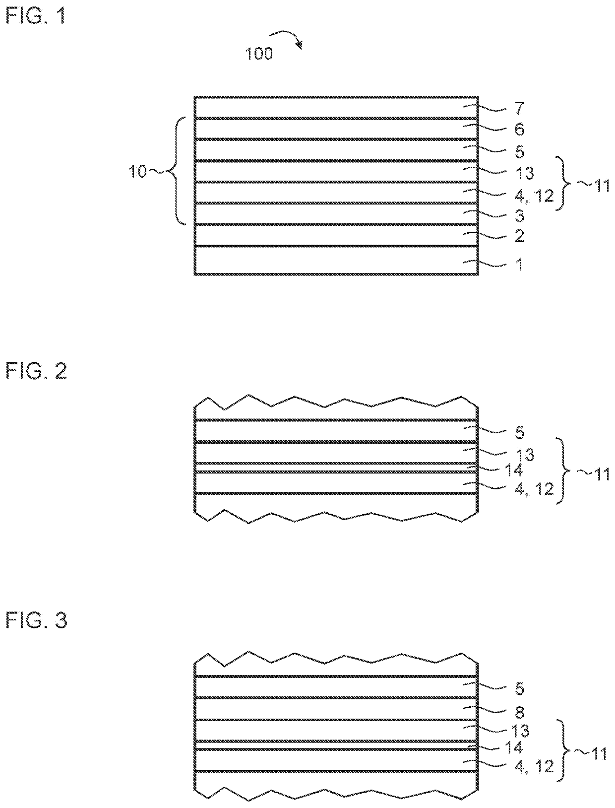
[0035]FIG. 1 shows an exemplary embodiment of an organic light-emitting component 100, which comprises an organic functional layer stack 10 having at least two organic light-emitting layers 4, 5 between two electrodes 2, 7.

[0036]In the exemplary embodiment shown, the electrodes 2, 7 and the organic functional layer stack 10 are arranged on a substrate 1. The substrate 1 can act as a carrier element for the layers applied thereon and comprise or be formed from, e.g., glass, for instance in the form of a glass film or glass sheet, quartz and / or a semiconductor material. Alternatively, the substrate 1 can also comprise or be formed from a plastic film or a laminate of multiple plastic films and / or glass films.

[0037]At least one of the two electrodes 2, 7 is transparent in form, wherein at least in the event that the organic light-emitting component 100 is in the form of a bottom emitter, in which the lower electrode 2 arranged between the substrate 1 and the organic functional layer st...


PUM

PropertyMeasurementUnit
thicknessaaaaaaaaaa
thicknessaaaaaaaaaa
thicknessaaaaaaaaaa

Abstract

An organic light-emitting component is disclosed. In an embodiment, the component includes an organic functional layer stack between two electrodes, wherein the organic functional layer stack comprises at least two organic light-emitting layers and at least one charge generation layer, and wherein at least one of the at least two organic light-emitting layers is part of the charge generation layer.

Description

[0001]This patent application is a national phase filing under section 371 of PCT / EP2016 / 052896, filed Feb. 11, 2016, which claims the priority of German patent application 10 2015 102 371.7, filed Feb. 19, 2015, each of which is incorporated herein by reference in its entirety.TECHNICAL FIELD[0002]An organic light-emitting component is provided.BACKGROUND[0003]An organic light-emitting diode (OLED) can convert pairs of charge carriers injected into an organic emitter layer to photons, each pair being formed from an electron and a hole. In an OLED with only one emitter layer, a maximum of one photon can be generated per pair of charge carriers injected. In order to achieve higher efficiency, it is known to stack multiple emitter layers one on top of another, wherein a charge generation layer (CGL) is arranged between adjacent emitter layers in each case. As a result, it may be possible to generate multiple photons per pair of charge carriers injected into such a stack, since the cha...

Claims


Application Information

Patent Timeline
Patent Type & Authority Patents(United States)
IPC IPC(8): H01L51/50H01L51/52C09K11/06H01L51/00
CPCC09K11/06H01L51/5278H01L51/5096H01L51/5024H01L51/0085C09K2211/1029H01L51/5056C09K2211/185H01L51/5072H10K50/12H10K50/19H10K50/13H10K50/18H10K50/15H10K50/16H10K85/342
Inventor PENTLEHNER, DOMINIKRAUSCH, ANDREASJAEGER, ARNDT
Owner DOLYA HOLDCO 5 LTD
Why Eureka
Try Eureka