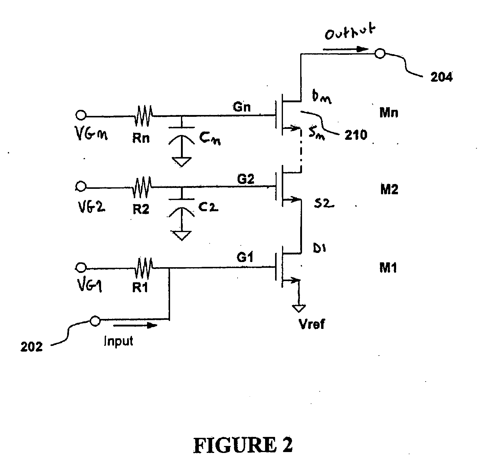
[0010]According to a first aspect, a power amplifier circuit is provided, comprising: a first
field effect transistor, wherein i) an RF input
signal terminal is adapted to be coupled to a gate
electrode of the first
field effect transistor and ii) a first
DC control voltage input is adapted to be coupled to the gate
electrode of the first
field effect transistor; one or more additional serially connected field effect transistors serially connected among themselves and to the first field effect
transistor, each having a source terminal connected to a drain terminal of a preceding field effect transistor, wherein one or more additional
DC control voltage inputs are each coupled to respective gate electrodes of the one or more additional field effect transistors, an output of the power amplifier circuit being taken on a drain
electrode of the last one of the one or more additional field effect transistors; and one or more capacitors, each coupled to a respective one of the one or more additional field effect transistors, wherein the first DC control voltage input, the one or more additional DC control voltage inputs and the one or more capacitors are selected to minimize generation of non-linearities of each field effect transistor of the power amplifier circuit and to maximize, through
phase alignment, cancellation of distortions between the field effect transistors of the power amplifier circuit whereby, upon minimization of non-linearities and maximization of cancellation of distortions, at least two of the first field effect transistor and the one or more additional field effect transistors are biased with different drain-source voltages Vds and / or different gate-source voltages Vgs.
[0011]According to a second aspect, a power amplifier comprising a plurality of amplifying components connected in parallel is provided, each amplifying component comprising: a) a first field effect transistor wherein a first DC control voltage input is adapted to be coupled to a gate terminal of the first field effect transistor; b) one or more additional serially connected field effect transistors serially connected among themselves and to the first field effect transistor, each having a source terminal connected to a drain terminal of a preceding field effect transistor, wherein one or more additional DC control voltage inputs are each coupled to respective gate terminals of the one or more additional field effect transistors; and c) one or more capacitors, each coupled to a respective one of the one or more additional field effect transistor wherein i) an RF input
signal terminal is adapted to be coupled to the gate terminal of the first field effect transistor of each amplifying component, thus providing the power amplifier with the same input to each amplifying component; ii) an output of the power amplifier is taken on the drain terminal of the last one of the one or more additional field effect transistors of each amplifying component, thus providing the power amplifier with the same output from each amplifying component; and iii) the first DC control voltage input, the one or more additional DC control voltage inputs and the one or more capacitors of at least one amplifying component are selected to minimize generation of non-linearities of each field effect transistor of the power amplifier circuit and to maximize, through
phase alignment, cancellation of distortions between the field effect transistors of the power amplifier whereby, upon minimization of non-linearities and maximization of cancellation of distortions, at least two of the first field effect transistor and the one or more additional field effect transistors of the at least one amplifying component are biased with different drain-source voltages Vds and / or different gate-source voltages Vgs.
[0012]According to a third aspect, a method for controlling
DC voltage inputs and
capacitance values of a power amplifier is provided, comprising: providing a first field effect transistor, wherein i) an RF input
signal terminal is adapted to be coupled to a gate electrode of the first field effect transistor and ii) a first DC control voltage input is adapted to be coupled to the gate electrode of the first field effect transistor; providing one or more additional serially connected field effect transistors serially connected among themselves and to the first field effect transistor, each having a source terminal connected to a drain terminal of a preceding field effect transistor, wherein one or more additional DC control voltage inputs are each coupled to respective gate electrodes of the one or more additional field effect transistors, an output of the power amplifier circuit being taken on a drain electrode of the last one of the one or more additional field effect transistors; providing one or more capacitors, each coupled to a respective one of the one or more additional field effect transistor; and controlling the first DC control voltage input, the one or more additional DC control voltage inputs and the one or more capacitors to minimize generation of non-linearities of each field effect transistor of the power amplifier circuit and to maximize, through
phase alignment, cancellation of distortions between the field effect transistors of the power amplifier circuit whereby, upon minimization of non-linearities and maximization of cancellation of distortions, at least two of the first field effect transistor and the one or more additional field effect transistors are biased with different drain-source voltages Vds and / or gate-source voltages Vgs.
[0013]According to a fourth aspect, a method for controlling
DC voltage inputs and
capacitance values of a power amplifier is provided, comprising: a) providing a first field effect transistor, wherein a first DC control voltage input is adapted to be coupled to a gate terminal of the first field effect transistor; b) providing one or more additional serially connected field effect transistors serially connected among themselves and to the first field effect transistor, each having a source terminal connected to a drain terminal of a preceding field effect transistor, wherein one or more additional DC control voltage inputs are each coupled to respective gate terminals of the one or more additional field effect transistors; and c) providing one or more capacitors, each coupled to a respective one of the one or more additional field effect transistor, wherein: i) an RF input signal terminal is adapted to be coupled to the gate terminal of the first field effect transistor of each amplifying component, thus providing the power amplifier with the same input to each amplifying component; and ii) an output of the power amplifier is taken on the drain terminal of the last one of the one or more additional field effect transistors of each amplifying component, thus providing the power amplifier with the same output from each amplifying component, the method further comprising d) controlling the first DC control voltage input, the one or more additional DC control voltage inputs and the one or more capacitors of at least one amplifying component to minimize generation of non-linearities of each field effect transistor of the power amplifier circuit and to maximize, through phase alignment, cancellation of distortions between the field effect transistors of the power amplifier whereby, upon minimization of non-linearities and maximization of cancellation of distortions, at least two of the first field effect transistor and the one or more additional field effect transistors of the at least one amplifying component are biased with different drain-source voltages Vds and / or gate-source voltages Vgs.
[0014]According to a fifth aspect, a
system for improving linearity of an
electronic circuit is provided, comprising: a sensor; a bias adjustment arrangement coupled to the sensor; a bias generator coupled to the bias adjustment arrangement; and an
electronic circuit coupled to the bias generator, the power amplifier adapted to receive an input signal and to provide an output signal to a load, wherein the bias adjustment arrangement controls bias values to be generated by the bias generator and fed to the
electronic circuit by reducing non-linearity of the output signal of the electronic circuit through action on parameters on which the non-linearity of the output signal depends.
[0015]According to a sixth aspect, a
system for improving linearity of a power amplifier is provided, comprising: a sensor; a bias adjustment arrangement coupled to the sensor; a bias generator coupled to the bias adjustment arrangement; and a power amplifier coupled to the bias generator, the power amplifier adapted to receive an input signal and to provide an output signal to a load, wherein the bias adjustment arrangement controls bias values to be generated by the bias generator and fed to the power amplifier by reducing non-linearity of the output signal of the power amplifier through action on parameters on which the non-linearity of the output signal depends, and wherein the power amplifier comprises the power amplifier defined in the previous second aspect above.


