Group iii nitride-based compound semiconductor light-emitting device and production method therefor

Active Publication Date: 2011-07-14
TOYODA GOSEI CO LTD
View PDF0 Cites 13 Cited by
  • Summary
  • Abstract
  • Description
  • Claims
  • Application Information

AI Technical Summary

Benefits of technology

[0042]According to the present invention, the protective layer comprising a group III nitride-based compound semiconductor whose band gap is larger than the barrier layer is formed just after forming the well layer comprising a semiconductor including at least In. For example, when the barrier layer consists of AlGaN, the layer whose Al composition ratio is higher than that of the barrier layer is employed for the protective layer. Even if the growth temperature for the barrier layer is set higher than that of the well layer, the protection of the well layer comprising In is stronger than that in case of the protective layer comprising GaN in the prior art. Because the protective layer having a high Al composition ratio is formed on the well layer and Al and N atomic binding is stronger than Ga and N atomic binding. Additionally, a film thickness of the protective layer comprising AlGaN whose Al composition ratio is high can be made to be thin compared with the protective layer comprising GaN of the prior art due to the strong Al and N atomic binding. This contributes to reduction in resistance of the quantum well structure such as a light-emitting layer or an active layer. Thus, it becomes possible to decrease the threshold voltage, i.e., the forward voltage, for operating the light-emitting device. And the film thickness of the protective layer comprising AlGaN whose Al composition ratio is high can be thinner compared with the film thickness of the protective layer comprising GaN of the prior art. Therefore, even if the protective layer is formed at the same low temperature as the well layer comprising In is formed at, a flatness of the surface does not become worse. Furthermore, the protective layer has a band gap larger than that of the barrier layer, which helps the barrier layer to confine carriers in the well layer.
[0043]This helps to improve light extraction performance of the Group III nitride-based compound semiconductor light-emitting device comprising the emitting layer or the active layer of the multiple quantum well structure.
[0044]Studies by the present inventors have shown that when an Al composition of the protective layer is high, distortion due to lattice mismatch between the protective layer and the well layer exert a bad influence on the protective layer. Consequently, the protective layer is preferable to be two-layered comprising, for example, the first protective layer comprising GaN formed directly on the well layer and the second protective layer comprising AlGaN formed on the first protective layer, which enables to achieve the sufficient effect of the present invention.

Problems solved by technology

However, when the semiconductor comprising Al is grown under less than 800° C., the semiconductor of high crystallinity can not be obtained.
However, when the well layer comprising In is epitaxially grown at the temperature of less than 800° C., then the barrier layer comprising Al is epitaxially grown at the temperature of equal to or more than 850° C., the barrier layer can not be grown in a succession of growth of the well layer.

Method used


Image

  • Group iii nitride-based compound semiconductor light-emitting device and production method therefor
  • Group iii nitride-based compound semiconductor light-emitting device and production method therefor

Examples


embodiment

[0059]Embodiments of the present invention will next be described with reference to the drawings. Characteristic features of the present invention described above are also the best mode for carrying out the invention, and the present invention is not limited to the below-described specific embodiments.

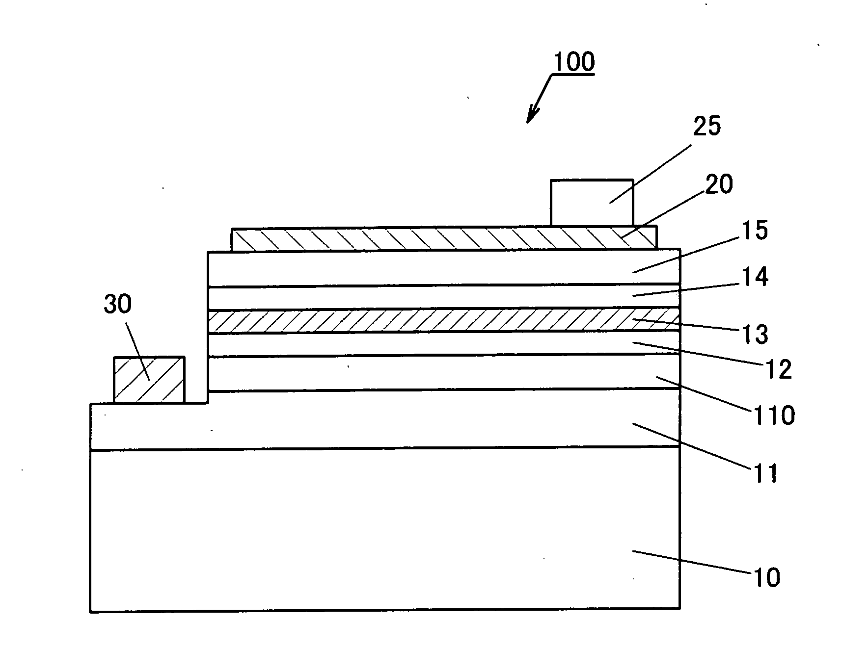
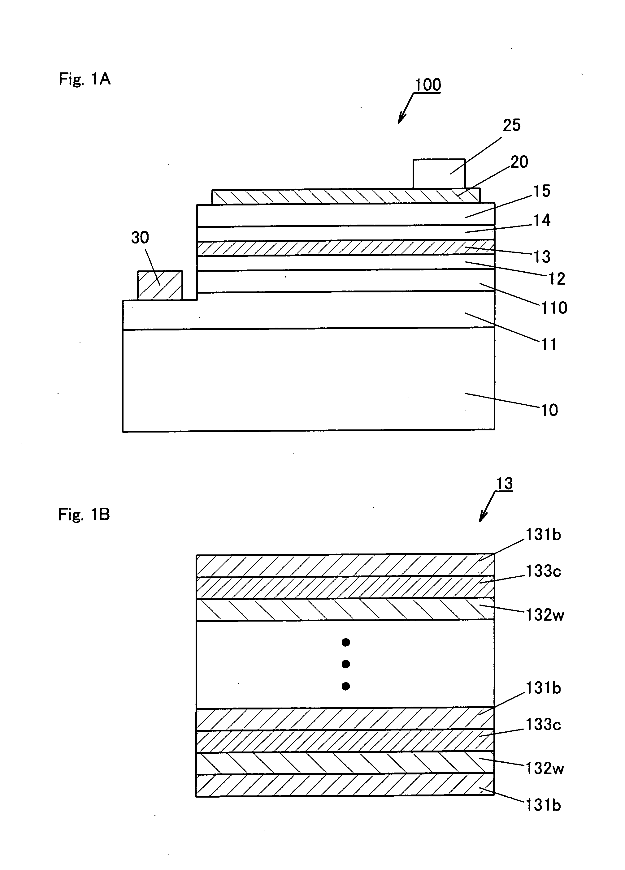
[0060]FIG. 1.A is a sectional view showing the construction of the group III nitride-based compound semiconductor light-emitting devices 100 with respect to eight examples of the present invention and a comparative example, which are produced for estimating the effect of the invention. The group III nitride-based compound semiconductor light-emitting devices 100 has an n contact layer 11 made of GaN doped with. silicon (Si) having thickness of about 4 μm. The n contact layer 11 is formed on a buffer layer having a thickness of about 15 nm comprising aluminum nitride (AlN), not shown, which is formed on a sapphire substrate 10. On the n contact layer 11, a multiple layer structure compr...


PUM


Abstract

The object of the present invention is to improve extraction efficiency of light of a Group III nitride-based compound semiconductor light-emitting device of a multiple quantum well structure. The device comprises a multiple quantum well structure comprising a well layer comprising a semiconductor including at least In for composition, a protective layer which comprises a semiconductor including at least Al and Ga for composition and has a band gap larger than a band gap of the well layer and is formed on and in contact with the well layer in a positive electrode side. And also the device comprises a barrier layer comprising a band gap which is larger than a band gap of the well layer and is smaller than a band gap of the protective layer, and formed on and in contact with the protective layer in a positive electrode side and a periodical structure of the well layer, the protective layer and the barrier layer.

Description

TECHNICAL FIELD[0001]The present invention relates to a group III nitride-based compound semiconductor light-emitting, device, and to a method for producing the device. As used herein, “Group III nitride-based compound semiconductor” encompasses a semiconductor represented by the formula AlxGayIn1-x-yN (0≦x≦1, 0≦y≦1, 0≦x+y≦1); such a semiconductor containing a predetermined element so as to attain, for example, an n-type / p-type conduction; and such a semiconductor in which a portion of a group III element is substituted by B or Tl, or a portion of the Group V element is substituted by P, As, Sb, or Bi.BACKGROUND ART[0002]A group III nitride-based compound semiconductor light-emitting devices whose light emitting layer or active layer have a multiple quantum well structure have been widely used as a light-emitting diode or a laser diode which emits a light with any spectrum in the range from purple to green.[0003]A multiple quantum well structure means, in principle, a periodical str...

Claims


Application Information

Patent Timeline
IPC IPC(8): H01L33/06H01L33/30
CPCH01L33/32H01L33/06
Inventor OKUNO, KOJI
Owner TOYODA GOSEI CO LTD
Why Eureka
Try Eureka