
Led light emitting apparatus and vehicle headlamp using the same

a technology of led light and headlamp, which is applied in the direction of lighting and heating apparatus, semiconductor/solid-state device details, etc., can solve the problems of reduced quantity of light emitted from led chips, and increased sub-mount substrate size b>211/b>, so as to reduce the inter-chip space, reduce the width of bonding areas, and reduce the size of the substra

Active Publication Date: 2011-06-09
TOYODA GOSEI CO LTD
View PDF3 Cites 31 Cited by
  • Summary
  • Abstract
  • Description
  • Claims
  • Application Information

AI Technical Summary

Benefits of technology

[0014]A first object of the invention is, in an LED light emitting apparatus with LED chips mounted on a substrate, to reduce the size of the substrate by reducing a width of bonding areas of conductive patterns on the substrate where wires are bonded and further, when the LED chips are disposed in a plurality of rows, to reduce an inter-chip-space between the rows of LED chips.
[0015]A second object of the invention is, in an LED light emitting apparatus with LED chips mounted on a substrate, to reduce electric resistance so as to make a voltage drop small by increasing a width of a common pattern for conductive patterns on the substrate.
[0016]A third object of the invention is, in a vehicle headlamp which employs an LED light emitting apparatus with LED chips mounted on a substrate and reflects to the front light emitted upwards from light emitting surfaces of the LED chips or to the peripheries thereof by a reflector, to prevent wires from entering optical paths directed from the LED chips towards the reflector to prevent the generation of shadows of the wires in the optical paths so as to eventually prevent a reduction in light quantity and deterioration of an external appearance of the headlamp.

Problems solved by technology

Because of this, a pattern width of the conductive pattern 213 where ends of the two wires 209, 209 are bonded is increased, leading to a problem that the size of the sub-mount substrate 211 is increased.
An inter-chip-space is increased because wires from one row are aligned with wires from the other row between the two rows of LED chips 201 in an end-to-end fashion, leading to a problem that the size of the sub-mount substrate 221 is also increased.
However, feeding terminals provided on a mounting holder of the illumination appliance are disposed at equal intervals, and their positions are determined and cannot be changed in many cases.
The shadow of the wire 209 then causes a problem that the quantity of light emitted from the LED chip 209 is reduced or an external appearance of the vehicle headlamp 240 is deteriorated as a result of the shadow being visible from an external location.

Method used


Image

  • Led light emitting apparatus and vehicle headlamp using the same
  • Led light emitting apparatus and vehicle headlamp using the same
  • Led light emitting apparatus and vehicle headlamp using the same

Examples


embodiment 1

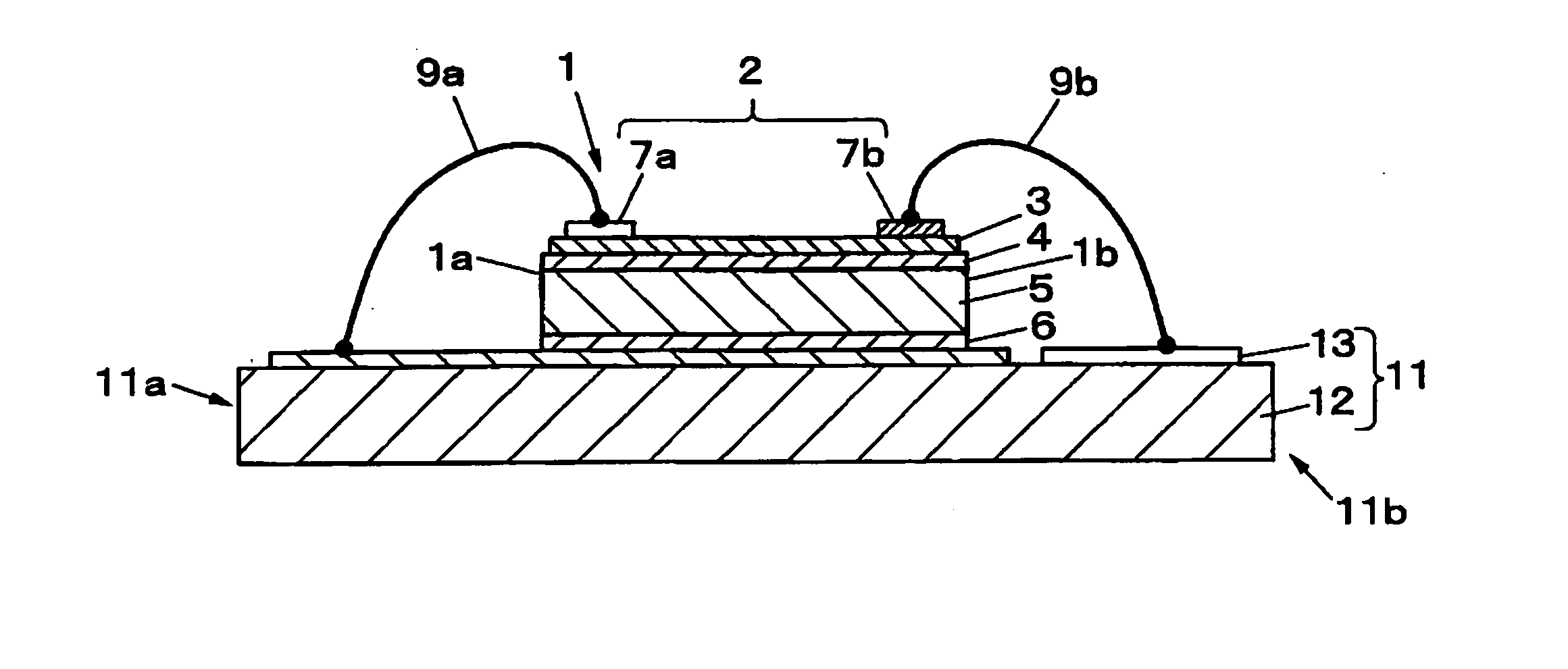
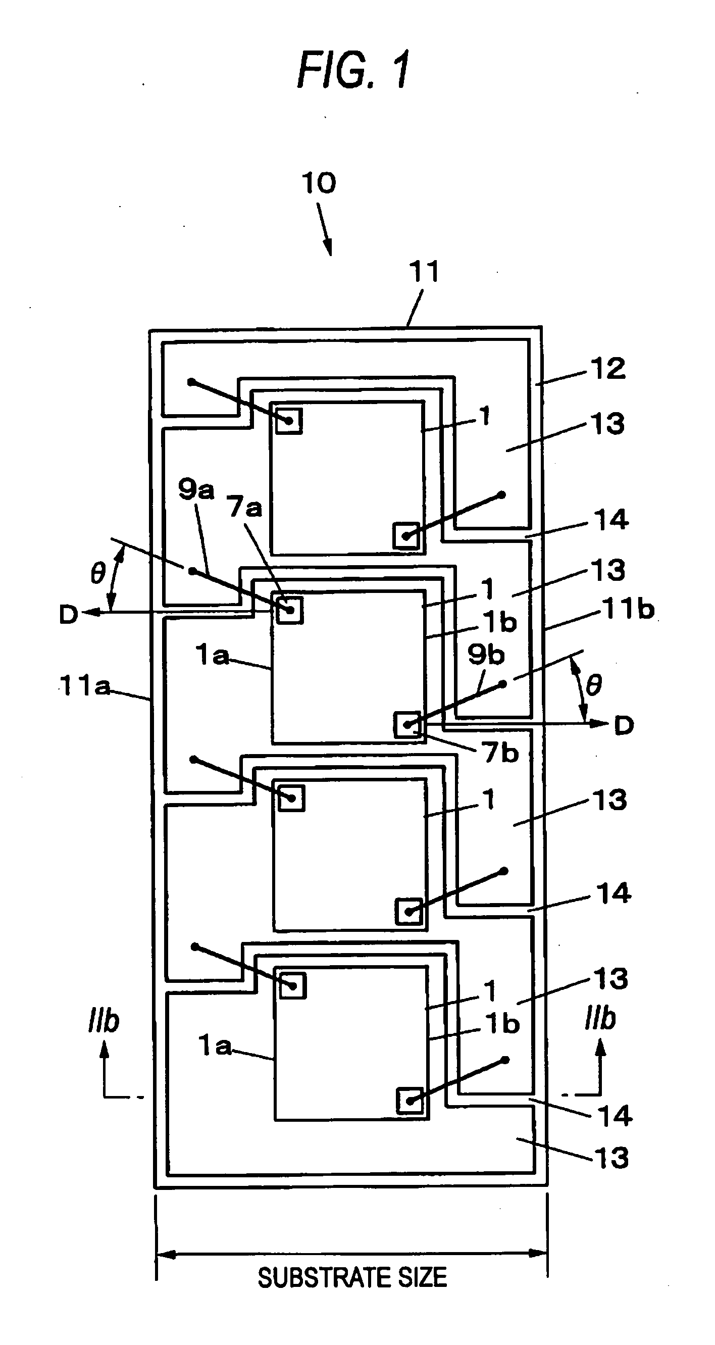
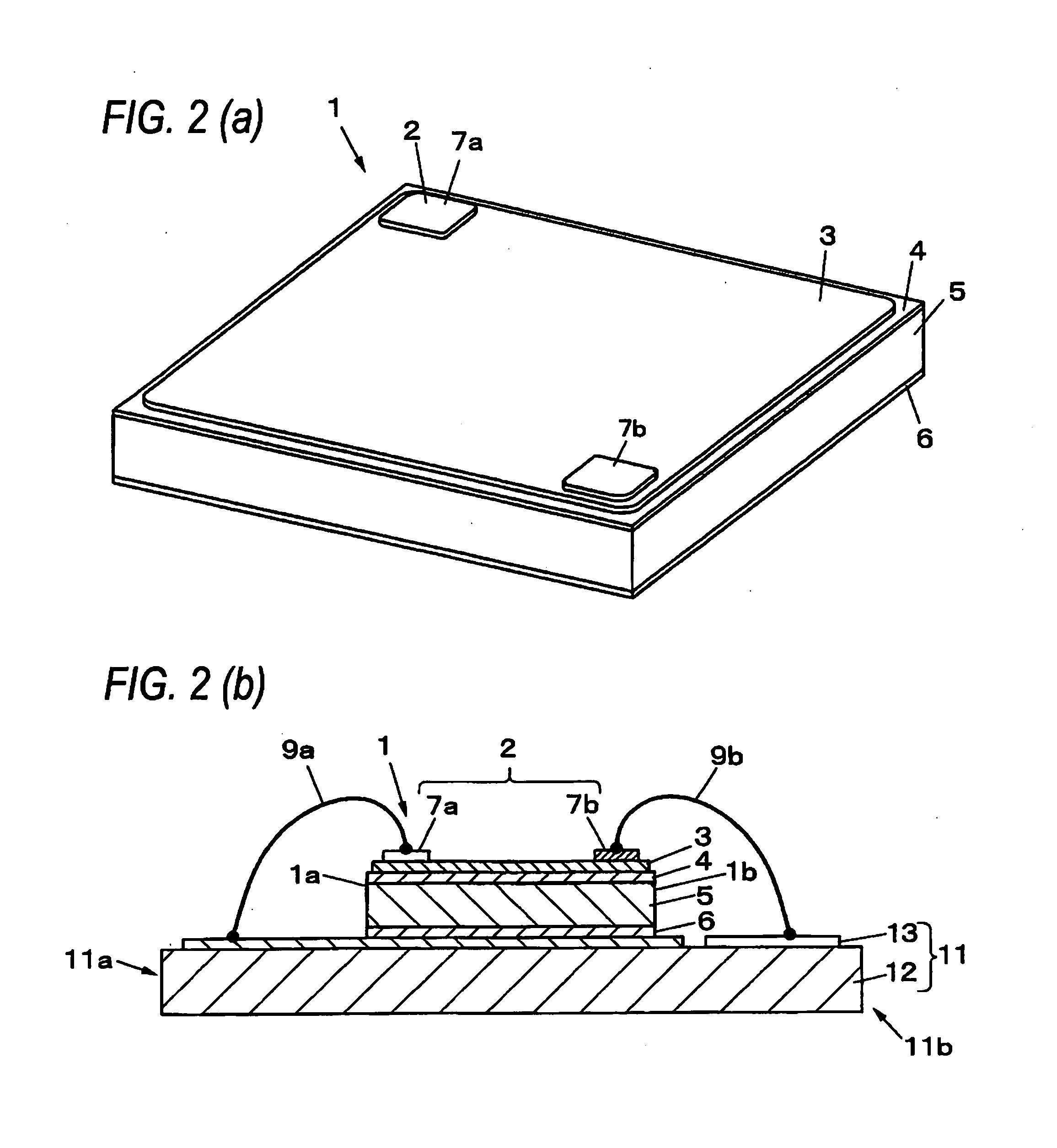
[0066]Embodiment 1 shown in FIGS. 1 and 2 is an LED light emitting apparatus 10 in which four LED chips are mounted into a single row on a sub-mount substrate 11 having a required minimum size to mount the four LED chips thereon so as to form a single series circuit.

[0067]LED chips each having a square shape of 1 mm by 1 mm as viewed from thereabove are used for the LED chips used in Embodiment 1. In FIG. 1, a first edge 1a and a second end 1b which face each other in a left-right direction are parallel. In addition, those fabricated by use of the LLO (Laser Lift Off) method are used as the LED chips. As is shown in FIG. 2, the LED chip includes sequentially from top to bottom an n electrode 2, a semiconductor layer 3, a conductive adhesive layer 4, a conductive substrate 5 and a p electrode layer 6. The semiconductor layer 3 includes sequentially from top to bottom an n-type cladding layer, a multiple quantum well type light emitting layer and a p-type cladding layer (whose illustr...

embodiment 2

[0074]Embodiment 2 shown in FIG. 3 is an LED light emitting apparatus 20 in which eight LED chips 1 are mounted on a sub-mount substrate 21 having a required minimum size to mount the eight LED chips 1 thereon into two rows so as to form two series circuits.

[0075]The LED chips 1 used in Embodiment 2 are the same as the LED chips 1 used in Embodiment 1. In FIG. 3, four LED chips 1 in a left row are referred to as first LED chips, and four LED chips 1 in a right row are referred to as second LED ships.

[0076]The sub-mount substrate 21 is a wiring board or printed circuit board which is made up of an insulating and highly heat conducting ceramic plate 22 (of aluminum nitride, for example) and conductive patterns 23 which are formed into wiring patterns on an upper surface of the ceramic plate 22. As viewed from thereabove, the sub-mount substrate 21 has a rectangular shape, and a first edge 21a and a second edge 21b, which face each other laterally in FIG. 3, are parallel. 10 conductive...

embodiment 3

[0085]Embodiment 3 shows in FIG. 4 is an LED light emitting apparatus 30 in which eight LED chips 1 are mounted in two rows so as to form two series circuits on a base substrate 31 which includes receiving terminals for contact with feeding terminals of an illumination appliance.

[0086]The LED chips 1 used in Embodiment 3 are the same as the LED chips 1 used in Embodiment 1.

[0087]The base substrate 31 is a wiring board or printed circuit board which is made up of an insulating and highly heat conducting ceramic plate 32 (of aluminum nitride, for example) and conductive patterns 33 which are formed into wiring patterns on an upper surface of the ceramic plate 32. As viewed from thereabove, the base substrate 31 has a rectangular shape, and a first edge 31a and a second edge 31b, which face each other laterally in FIG. 4, are parallel. A third edge or an upper edge of the base substrate 31 constitutes a mounting edge where the LED light emitting apparatus 30 is mounted on an illuminati...


PUM


Abstract

Four LED chips are mounted on a sub-mount substrate so as to be parallel thereto. A wire 9a is installed to extend between a pad electrode 7a of two pad electrodes 7a, 7b provided in two diagonal corners of an upper surface of the LED chip 1 which pad electrode 7a is disposed on a first edge 1a side of the LED chip 1 and a bonding area of a conductive pattern 13 so as to be inclined at 15 to 40 degrees towards an orientation which moves away from a first edge 1a with respect to an orthogonal moving-away direction D relative to the first edge 1a. A wire 9b is installed to extend between the pad electrode 7b which is disposed on a second edge 1b side of the LED chip 1 and a bonding area of the conductive pattern 1 so as to be inclined 15 to 40 degrees towards an orientation which approaches a second edge 1b of the LED chip 1 with respect to an orthogonal moving-away direction D relative to the second edge 1b.

Description

BACKGROUND[0001]1. Field of the Invention[0002]The present invention relates to an LED light emitting apparatus in which LED chips are mounted on a substrate and a vehicle headlamp using the same.[0003]2. Description of the Related Art[0004]Enlarging LED chips (500 μm to 1 mm long on one edge) is propagated to allow a large current to flow for high light output and / or to cause them to be driven in low-current regions of high luminous efficiency by reducing a current density per area, and a plurality of pad electrodes for wire bonding are formed on a wide area of light emitting surface of such an LED chip for uniform current supply (Patent Documents 1, 2).[0005]A conventional example 1 shown in FIG. 15 is an LED light emitting apparatus 210 in which four large LED chips 201 are mounted on a sub-mount substrate of a required minimum size for mounting the LED chips 201 in a row to form a single series circuit. Formed on a light emitting surface of the LED chip 201 are two pad electrode...

Claims


Application Information

Patent Timeline
IPC IPC(8): H01L33/62
CPCF21S48/1109H01L2924/15151F21S48/1163H01L25/0753H01L33/62F21S48/1159H01L2224/73265H01L2224/48227H01L2924/01322H01L2224/92247H01L2224/45144H01L2224/48091H01L2924/00014H01L2924/00F21S41/148F21S41/151F21S41/155F21S41/192
Inventor HAKAMATA, SHINTAROMINATO, TATSUYA
Owner TOYODA GOSEI CO LTD
Learn More