Resist pattern thickening material, semiconductor device, and production method thereof

a technology of resist pattern and thickening material, which is applied in the direction of solid-state devices, medical preparations, granular delivery, etc., can solve the problems of low throughput of resist pattern, high cost of updating, and inability to meet low-cost mass production, etc., and achieve the effect of thickening resist pattern

Inactive Publication Date: 2011-05-05
FUJITSU LTD
View PDF6 Cites 5 Cited by
  • Summary
  • Abstract
  • Description
  • Claims
  • Application Information

AI Technical Summary

Benefits of technology

[0015]According to another aspect of the invention, a method for producing a semiconductor device contains applying the aforementioned resist pattern thickening material to a resist pattern formed on a processing surface so as to cover a surface of the resist pattern with the resist pattern thickening material to thereby thicken the resist pattern.

Problems solved by technology

However, the exposure technique using this electron beam has problems such that the through-put thereof is low and it is not suitable for a low-cost mass-production.
However, to shorten the wavelength of the light source of the exposure device, it is necessary to update the exposure device, and thus a significant amount of the cost is expected for the updating.
However, the improvement of the resist material has a limitation, and it is extremely difficult to satisfy all the required properties for the resist material.
However, the resist pattern thickening material used for RELACS has a problem such that it does not work on an ArF resist pattern formed by exposing an ArF resist film to ArF (argon fluoride) excimer laser light (a wavelength of 193 nm) that is currently used for a fine processing technique.
Accordingly, it is difficult to apply such the resist pattern thickening material in the practical use.
For a material for forming a semiconductor in the form of a coating solution, the defects caused by the re-deposition of sublimates are problems in the production, such as lowing yields or lowing performance of a final product (see, for example, JP-A Nos. 2005-165096 and 2007-114245).

Method used


Image

  • Resist pattern thickening material, semiconductor device, and production method thereof
  • Resist pattern thickening material, semiconductor device, and production method thereof
  • Resist pattern thickening material, semiconductor device, and production method thereof

Examples


example 1

Preparation of the Resist Pattern Thickening Material

[0149]The resist pattern thickening materials A to Q each having the formulation depicted in Table 1 were prepared.

[0150]Note that, in Table 1, “a thickening material” means a resist pattern thickening material; and “A” to “Q” are corresponded to the resist pattern thickening materials A to Q. Among the resist pattern thickening materials A to Q, the resist pattern thickening materials A, B, P and Q are comparative examples, and the resist pattern thickening materials C to O are examples (the embodiments of the invention). In Table 1, the unit for the value written in the parenthesis represents “mass (g)”.

[0151]The cyclodextrin compound of any of the resist pattern thickening materials C to O in the columns of “Compound expressed by general formula 1” is the cyclic compound expressed by the general formula 1. The cyclic compound expressed by the general formula 1 was added to each resist pattern thickening material in an amount of...

example 2

Production of a Semiconductor Device

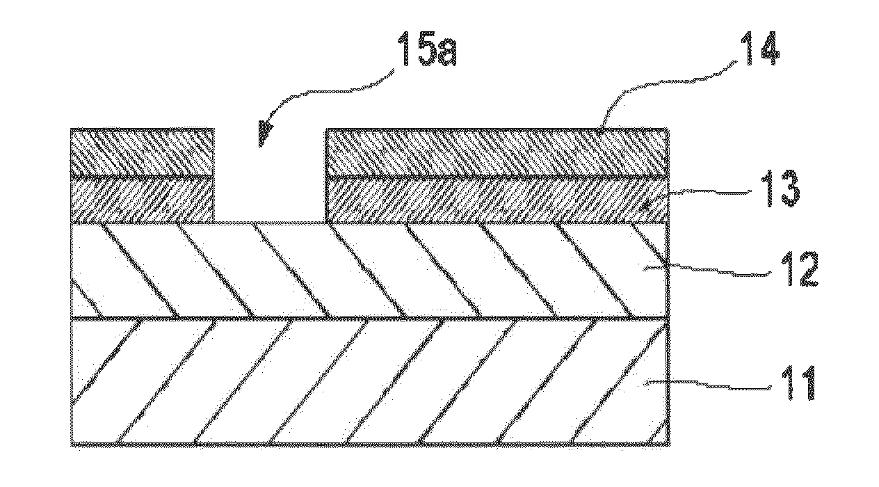
[0169]As illustrated in FIG. 4A, an interlayer insulating film 12 was formed on a silicon substrate 11, and as illustrated in FIG. 4B, a titanium film 13 was formed on the interlayer insulating film 12 by sputtering. Then, as illustrated in FIG. 4C, a resist pattern 14 was formed by a double patterning method, and the titanium film 13 was patterned by a reactive ion etching using the resist pattern 14 as a mask to thereby form an opening 15a. As well as sequentially removing the resist pattern 14 by the reactive ion etching, as illustrated in FIG. 4D, an opening 15b was formed in the interlayer insulating film 12 using the titanium film 13 as a mask. Then, the titanium film 13 was removed by a wet treatment, and as illustrated in FIG. 4E, a TiN film 16 was formed on the interlayer insulating film 12 by sputtering, followed by forming a Cu film 17 on the TiN film 16 by electroplating. Thereafter, as illustrated in FIG. 4F, the surface was flattened...


PUM

PropertyMeasurementUnit
Fractionaaaaaaaaaa
Fractionaaaaaaaaaa
Fractionaaaaaaaaaa

Abstract

A resist pattern thickening material containing a resin, a cyclic compound expressed by the general formula 1, at least one of compounds expressed by the general formulae 2 to 3, respectively, and water:

Description

CROSS-REFERENCE TO RELATED APPLICATIONS[0001]This application is based upon and claims the benefits of the priority of the prior Japanese Patent Application No. 2009-252800, filed on Nov. 4, 2009, the entire contents of which are incorporated herein by reference.FIELD[0002]The embodiments discussed herein relate to a resist pattern thickening material, a semiconductor device produced by using such the material, and a production method of such the device.BACKGROUND[0003]The formation of fine patterns has been desired for semiconductor devices such as a semiconductor integrated circuit (LIS: Large Scale Integration) along with the improvements in the integration degree, and the minimum pattern has been currently reached the size of 100 nm or smaller.[0004]The formation of such fine patterns in a semiconductor device is realized by an exposure technique using an electron beam capable of forming a fine pattern in the size of 100 nm or smaller. However, the exposure technique using this ...

Claims


Application Information

Patent Timeline
IPC IPC(8): H01L29/02C08L5/00H01L21/311
CPCC08L5/16C08L29/04C09D105/16C09D129/04G03F7/40H01L21/0273H01L21/76816H01L21/31144C08L31/04C08L39/06
Inventor KOZAWA, MIWANOZAKI, KOJI
Owner FUJITSU LTD
Why Eureka
Try Eureka