Semiconductor laser device
- Summary
- Abstract
- Description
- Claims
- Application Information
AI Technical Summary
Benefits of technology
Problems solved by technology
Method used
Image

Examples
first embodiment
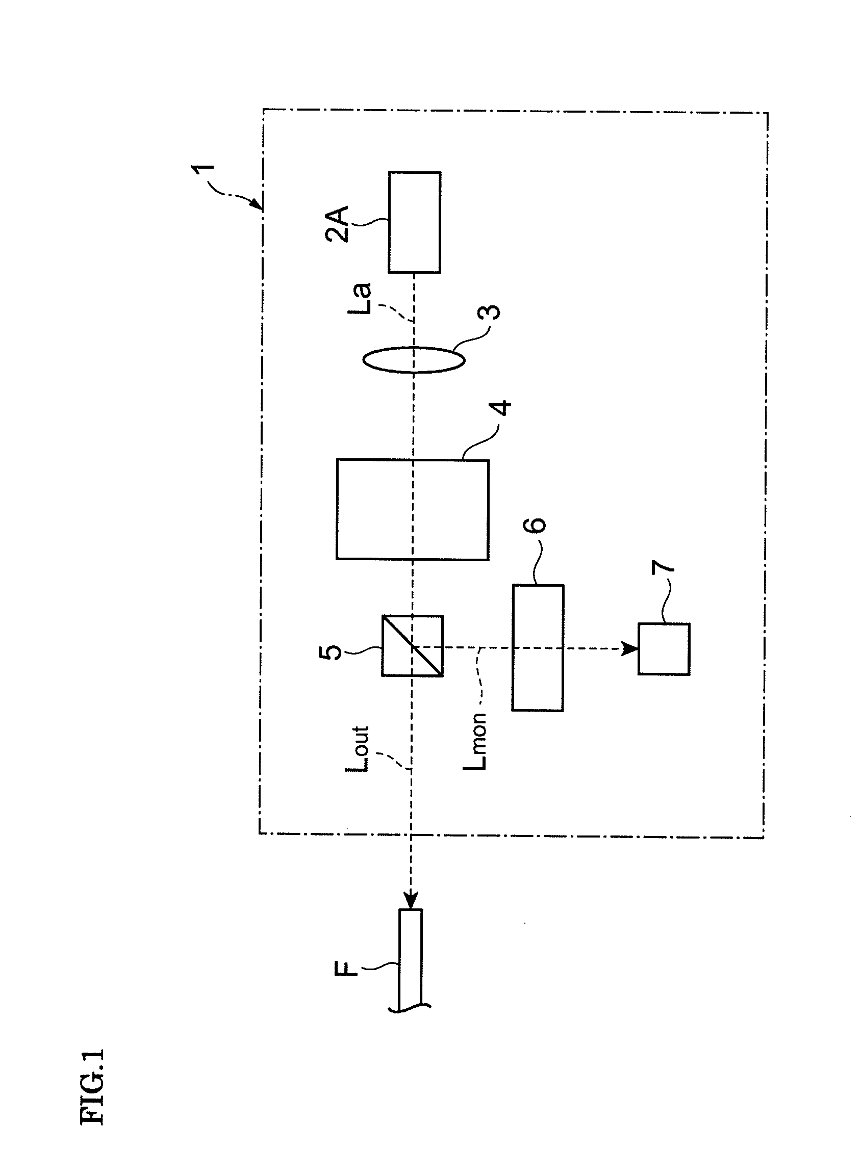
[0047]A semiconductor laser device according to a first embodiment of the present invention will now be described. Referring to FIG. 1, a semiconductor laser device 1 according to this embodiment includes a semiconductor laser 2A, a lens 3, an optical isolator 4, a beam splitter 5, an etalon filter 6, and a photodiode element 7.
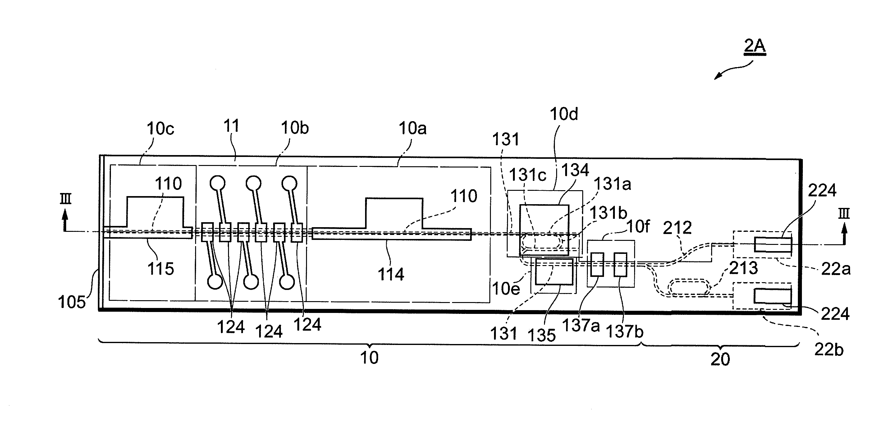
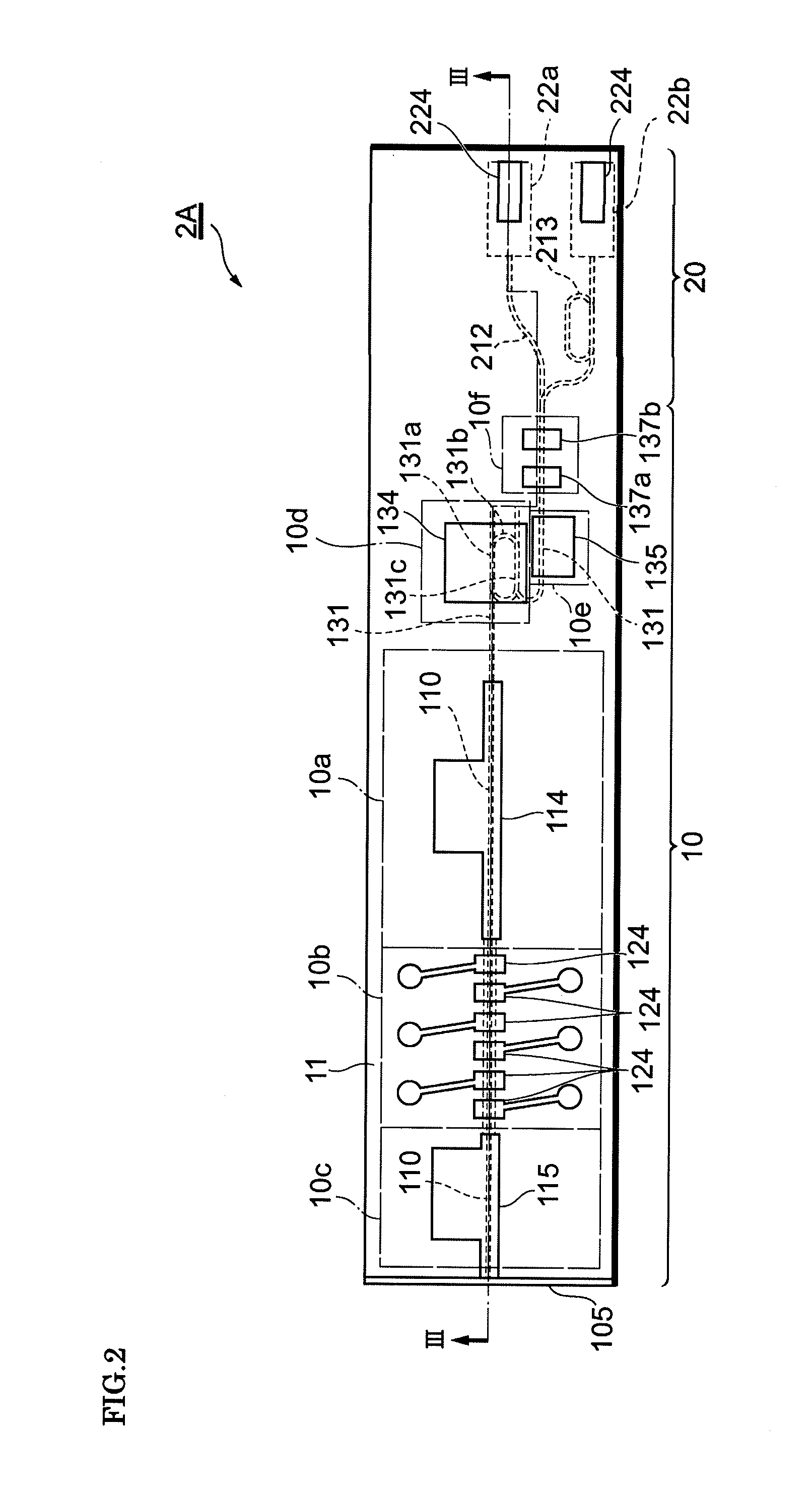
[0048]The semiconductor laser 2A is formed by integrating a wavelength-tunable semiconductor laser region (laser diode) that generates a laser beam La of any wavelength, and a wavelength-monitoring region for monitoring the wavelength of the laser beam La on a single semiconductor substrate.
[0049]The lens 3 is an optical component for collimating the laser beam La emitted from the semiconductor laser 2A and is optically coupled to a light-emitting end of the semiconductor laser 2A. The optical isolator 4 is an optical component for removing reflected light of the laser beam La returned to the semiconductor laser 2A. An input end of the optical isolator 4 is o...
second embodiment
[0118]Next, a semiconductor laser device according to a second embodiment of the present invention will now be described. Among the structures of the semiconductor laser device of this embodiment, the structures other than the structure of a semiconductor laser are the same as those in the first embodiment. Therefore, a detailed description of the common structures is omitted.
[0119]Referring to FIGS. 13 and 14, a semiconductor laser 2B of this embodiment includes a semiconductor laser region 40 functioning as a laser diode and a wavelength-monitoring region 20. The semiconductor laser region 40 has a distributed feedback (DFB) laser structure and includes a DFB laser region 40a and a coupling region 40b. The coupling region 40b is provided in order to optically couple the DFB laser region 40a to the wavelength-monitoring region 20. The structure and the function of the wavelength-monitoring region 20 are the same as those of the first embodiment.
[0120]As shown in FIG. 14, the semico...
third embodiment
[0129]Next, a semiconductor laser device according to a third embodiment of the present invention will be described. In this embodiment, the structures other than the structure of a semiconductor laser are the same as those in the first embodiment. Therefore, a detailed description of the common structures is omitted.
[0130]Referring to FIG. 16, a semiconductor laser 2C of this embodiment includes a semiconductor laser region 50 functioning as a laser diode and a wavelength-monitoring region 60. Although not shown in the figure, the semiconductor laser region 50 and the wavelength-monitoring region 60 are formed on a single semiconductor substrate. Furthermore, the semiconductor laser 2C is mounted on a temperature control device having the same structure as that of the temperature control device 30 shown in FIG. 3.
[0131]The semiconductor laser region 50 of this embodiment differs from the semiconductor laser region 10 of the first embodiment in the reflection structure on the end fa...
PUM
 Abstract
Description
Claims
Application Information
 - R&D
- Intellectual Property
- Life Sciences
- Materials
- Tech Scout
- Unparalleled Data Quality
- Higher Quality Content
- 60% Fewer Hallucinations
Browse by: Latest US Patents, China's latest patents, Technical Efficacy Thesaurus, Application Domain, Technology Topic, Popular Technical Reports.
© 2025 PatSnap. All rights reserved.Legal|Privacy policy|Modern Slavery Act Transparency Statement|Sitemap|About US| Contact US: help@patsnap.com