Silicon epitaxial wafer and method for production thereof
- Summary
- Abstract
- Description
- Claims
- Application Information
AI Technical Summary
Benefits of technology
Problems solved by technology
Method used
Image
Examples
first embodiment
[0022]The best mode of product according to the present embodiment may be obtained through growing an epitaxial layer on a silicon single crystal substrate having a {110} plane as the main surface, the off-angle thereof being less than one degree, and thereafter polishing the surface of the epitaxial layer.
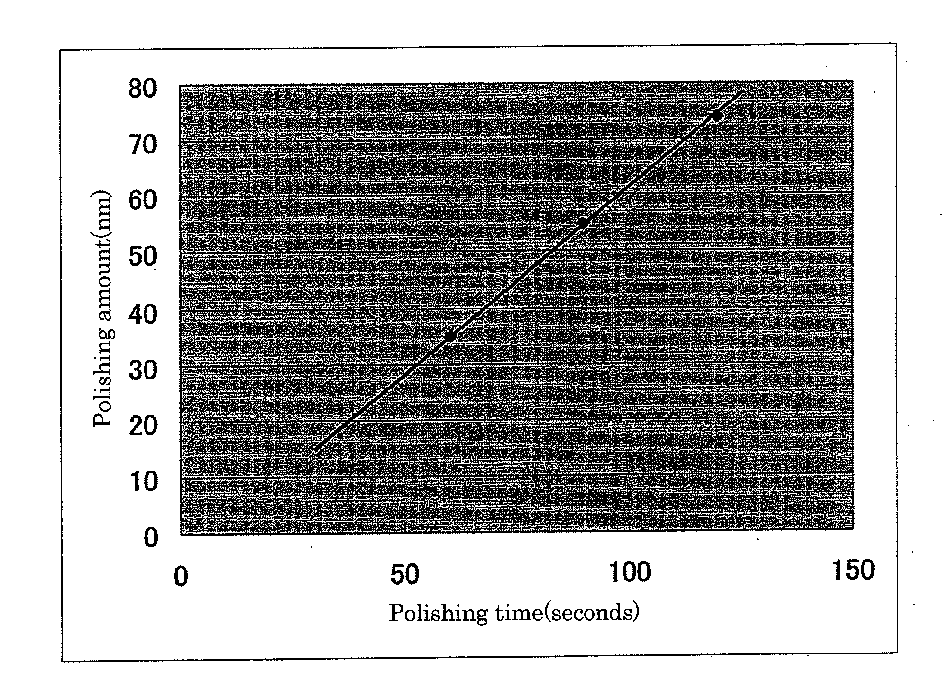
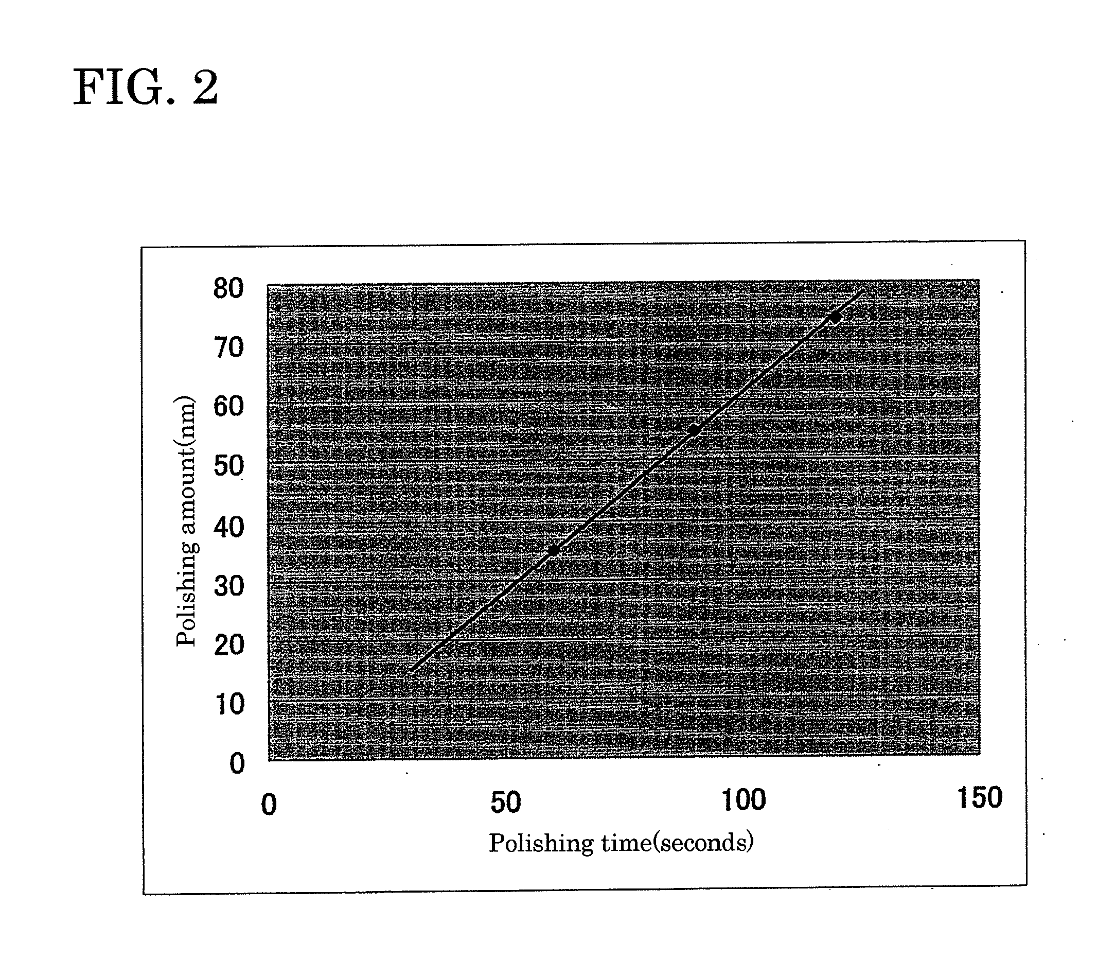
[0023]The polishing depth may be required as being 0.05 μm or more from a view point of improving the haze level. Although the upper limit thereof is not particularly limited, it may be sufficient to be 1 μm or less in the same view point.
example 1
[0024]A p-type silicon single crystal ingot was produced with the main axis orientation of and the diameter of 305 mm through the CZ method. After periphery grinding the ingot into 300 mm diameter and then notching, a plurality of blocks having electrical resistivity within the range of 5 to 10 mΩcm were cut out from the ingot. The blocks were sliced using wire saw into wafers with inclination orientations , , and of the {110} plane each having off-angles 0 degree to 10 degrees relative to each orientation, as shown in Table 1.
[0025]Mirror polished wafers were obtained from the sliced wafers after processing through corner rounding, lapping, finishing corner rounding, etching, both surfaces polishing, tape corner rounding, minor polishing of edges, and one surface polishing of top surfaces, in this order. Although cleaning treatments between the above processes are omitted to be described, the wafers were cleaning treated in a similar way as a conventional wafer working process.
[0...
second embodiment
[0031]Incidentally, epitaxial wafers have been used as materials for high performance devices because of the completeness in crystalline structure thereof. In accordance with miniaturization in device production processes during recent years, surface flatness and purity of epitaxial wafers are more severely demanded than ever before. To this end, known in the art is a method of polishing the surface after epitaxially growing (refer to Japanese Patent Application Publication 2006-120939, for example).
[0032]However, the wafer epitaxially processed in such a method is possibly to have been significantly deteriorated in haze level of the wafer surface when treated by polishing. If the haze level is high, then LPD is unable to be measured using a surface inspection system, and therefore the quality may not be evaluated.
[0033]Given the foregoing, the object of the present embodiment is to provide a method for producing a silicon epitaxial wafer free from an abnormal phenomenon that the ha...
PUM
 Abstract
Description
Claims
Application Information
 - R&D
- Intellectual Property
- Life Sciences
- Materials
- Tech Scout
- Unparalleled Data Quality
- Higher Quality Content
- 60% Fewer Hallucinations
Browse by: Latest US Patents, China's latest patents, Technical Efficacy Thesaurus, Application Domain, Technology Topic, Popular Technical Reports.
© 2025 PatSnap. All rights reserved.Legal|Privacy policy|Modern Slavery Act Transparency Statement|Sitemap|About US| Contact US: help@patsnap.com


